
Image taking device and camera system

a technology of image taking device and camera system, which is applied in the direction of exposure control, optical radiation measurement, instruments, etc., can solve the problems of narrow dynamic range of measurement process, high cost of system employing photon counter, and raised problems in taking process as described above, so as to reduce pixel aperture ratio and large dynamic range. , the effect of small nois

Active Publication Date: 2013-07-23
SONY SEMICON SOLUTIONS CORP
View PDF8 Cites 64 Cited by
  • Summary
  • Abstract
  • Description
  • Claims
  • Application Information

AI Technical Summary

Benefits of technology

The patent invention allows for measuring light and taking pictures at a high dynamic range without reducing the amount of light coming through the camera. This is done by processing signals in a way that reduces the amount of noise and introduces only a small amount of error at low light levels.

Problems solved by technology

On the other side of the coin, however, a system employing the photon counter is expensive and the dynamic range of a measurement process is narrow.
However, the image taking process as described above raises problems.
One of the problems is noises generated in propagation of the analog signal.
Another problem is the speed of the AD converter.
Thus, the size of a system for AD conversion is very large.
However, there is no device that meets both of these requirements.
By making use of an ordinary photon counter, however, a dynamic range sufficient for the image taking operation is not satisfied.
However, such a system is extremely expensive.
In accordance with the technology disclosed in Patent Document 1, however, every pixel requires a sense circuit and a counter so that the aperture area of the pixel inevitably becomes very small.
Thus, the circuit size of a chip including the counters is unavoidably large.

Method used


Image

  • Image taking device and camera system
  • Image taking device and camera system
  • Image taking device and camera system

Examples


first embodiment

2. First Embodiment

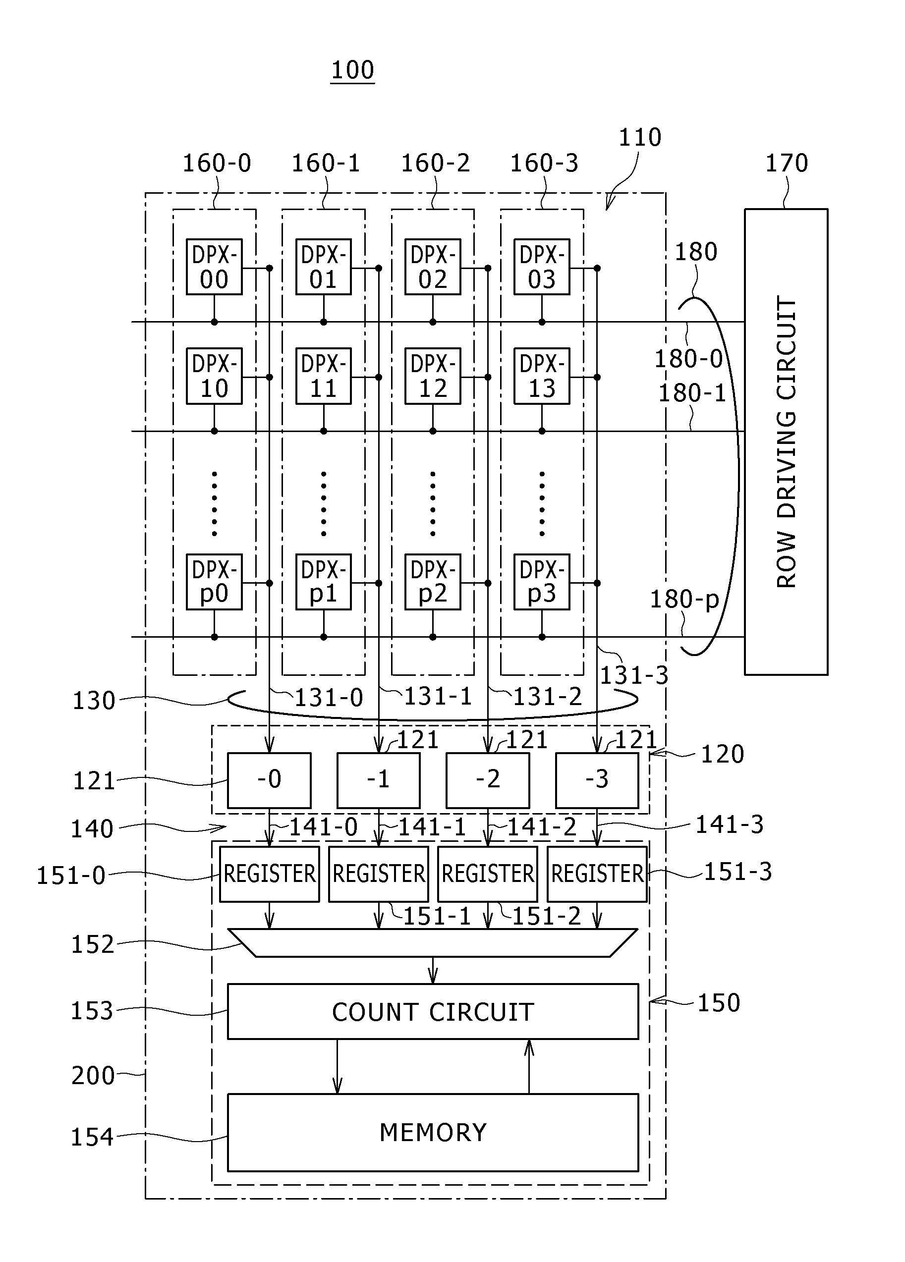
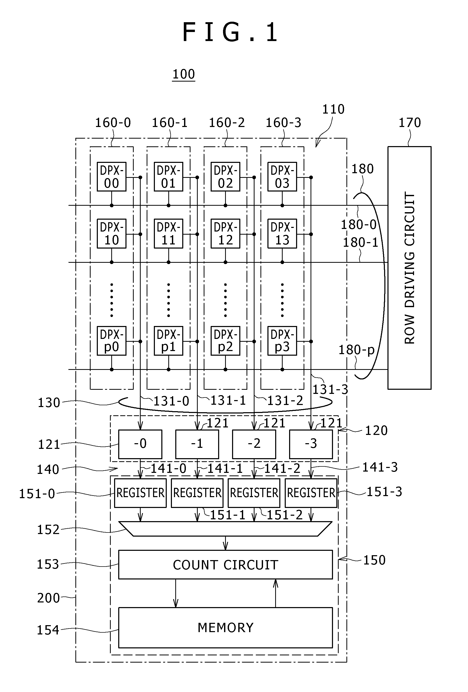
[0072]FIG. 1 is a block diagram showing a configuration of a CMOS image sensor 100 serving as an image taking device according to a first embodiment of the present invention.

Outline of the Entire Configuration

[0073]As shown in the figure, the CMOS image sensor 100 employs a pixel array section 110, a sense circuit section 120, an output-signal line group 130, a transfer line group 140 and a determination-result integration circuit section 150.

[0074]As will be described later, in the CMOS image sensor 100, a plurality of pixels share one sense circuit.

[0075]In addition, in the CMOS image sensor 100, each plurality of pixels DPX pertaining to a column and a pixel select circuit (not shown in the drawing) for selecting one of the pixels DPX from one of pixel blocks 160-0, 160-1, 160-3 and so on.

[0076]On top of that, the CMOS image sensor 100 has a row driving circuit 170 and a row control line group 180. The row driving circuit 170 is a section for driving each pixel...

second embodiment

3. Second Embodiment

[0235]The following description explains a second embodiment which implements a configuration of applying the photodiode having an embedded internal amplifier to a light receiving apparatus.

[0236]FIG. 8 is an explanatory diagram showing a configuration of pixel blocks each provided with an internal-amplifier photodiode in accordance with the second embodiment of the present invention to serve as a counterpart of a pixel block according to the first embodiment.

[0237]In the case of the second embodiment, the pixel block 160B is configured as a group of pixels DPXB which each include only an internal-amplifier photodiode 111B and a transport (select) transistor 112B for the internal-amplifier photodiode 111B.

[0238]That is to say, every pixel DPXB is configured to include only an internal-amplifier photodiode 111B and a transfer (select) transistor 112B for the internal-amplifier photodiode 111B. The gate electrodes of the transfer (select) transistors 112B employed ...

third embodiment

4. Third Embodiment

[0241]The following description explains a third embodiment which implements a configuration of an image taking apparatus making use of a plurality of light receiving apparatus each based on an image taking device according to the first or second embodiment. Each of the light receiving apparatus employs a light receiving section and circuit blocks.

[0242]The semiconductor image taking apparatus represented by sensors including the ordinary CCD (Charge Coupled Device)-type image taking sensor and the ordinary CMOS image sensor has characteristic variations of an amplifier circuit at the CCD output section and characteristic variations of a source follower circuit pertaining to every pixel in the CMOS image sensor.

[0243]In the ordinary semiconductor image taking apparatus, the characteristic variations are reflected as they are in variations of the efficiency of a process to convert the number of accumulated photons into an analog electrical signal.

[0244]In addition,...


PUM


Abstract

An image sensor includes a plurality of pixels, a plurality of sense circuits, and a count circuit. Each sense circuit is configured to read out electrical signals from at least one pixel associated with the sense circuit in order to generate data representing whether or not photons have been received by the sense circuit. The count circuit is in communication with a sense circuit selected from the plurality of sense circuits. The count circuit is configured to provide integration results for the pixels associated with the sense circuits based on the data received from the sense circuits.

Description

RELATED APPLICATION DATA[0001]The present application claims priority to Japanese Priority Patent Application JP 2009-229893 filed in the Japan Patent Office on Oct. 1, 2009, which is incorporated by reference in its entirety to the extent permitted by law.BACKGROUND OF THE INVENTION[0002]The present invention relates to image taking devices such as a CMOS (Complementary Metal Oxide Semiconductor) image sensors and camera systems employing same.[0003]In recent years, techniques for measuring minute amounts of light emitted by or from a biological body and fluorescent light, as well as techniques for taking images, have been developed in the fields of medical cares and biotechnologies.[0004]In addition, a transmission image taking technology has been applied to products in the medical-care and security fields. In accordance with the transmission image taking technology, few X rays passing through an object of observation are converted by a scintillator into photons at the visible lev...

Claims


Application Information

Patent Timeline
Patent Type & Authority Patents(United States)
IPC IPC(8): H04N3/14
CPCH04N5/32H04N5/357H04N5/355H04N5/3355H04N25/57H04N25/671H04N23/30H04N25/618H04N25/65H04N25/533H04N25/78H04N25/773H04N25/00H04N25/772H04N25/60H04N25/75H04N25/767G01J1/44G01J2001/444
Inventor NISHIHARA, TOSHIYUKI
Owner SONY SEMICON SOLUTIONS CORP
Learn More