Display substrate, method of manufacturing the display substrate, and display device having the display substrate

a technology of display substrate and manufacturing method, which is applied in the direction of instruments, polarising elements, optics, etc., can solve the problems of absorbing, reducing the light density of the display device, and dispersing a large amount of light, so as to reduce the cost of manufacturing a display device, shorten the pathway of light, and reduce the loss of light

Inactive Publication Date: 2013-08-06
SAMSUNG DISPLAY CO LTD
View PDF26 Cites 1 Cited by
  • Summary
  • Abstract
  • Description
  • Claims
  • Application Information

AI Technical Summary

Benefits of technology

[0008]In one aspect, the present invention provides a display device for simplifying a structure to improve optical efficiency.
[0031]According to some example embodiments of the present invention, a combination of the first, second and third nano metal wires, and the first and second dielectric layers may generate surface plasmon resonance and induce polarized color light. Therefore, a conventional color filter and a conventional lower polarization plate may be omitted, so that a cost of manufacturing a display device may be reduced. Furthermore, the simplified structure may shorten a pathway of light and reduce a loss of the light, so that optical efficiency may be improved.

Problems solved by technology

However, the light emitted from the backlight unit passes via various elements such as a polarization plate disposed outside the LCD panel, signal lines, a color filter, a liquid crystal layer, etc., such that a considerable amount of the light is dispersed, absorbed, or reflected.

Method used


Image

  • Display substrate, method of manufacturing the display substrate, and display device having the display substrate
  • Display substrate, method of manufacturing the display substrate, and display device having the display substrate
  • Display substrate, method of manufacturing the display substrate, and display device having the display substrate

Examples


exemplary embodiment 1

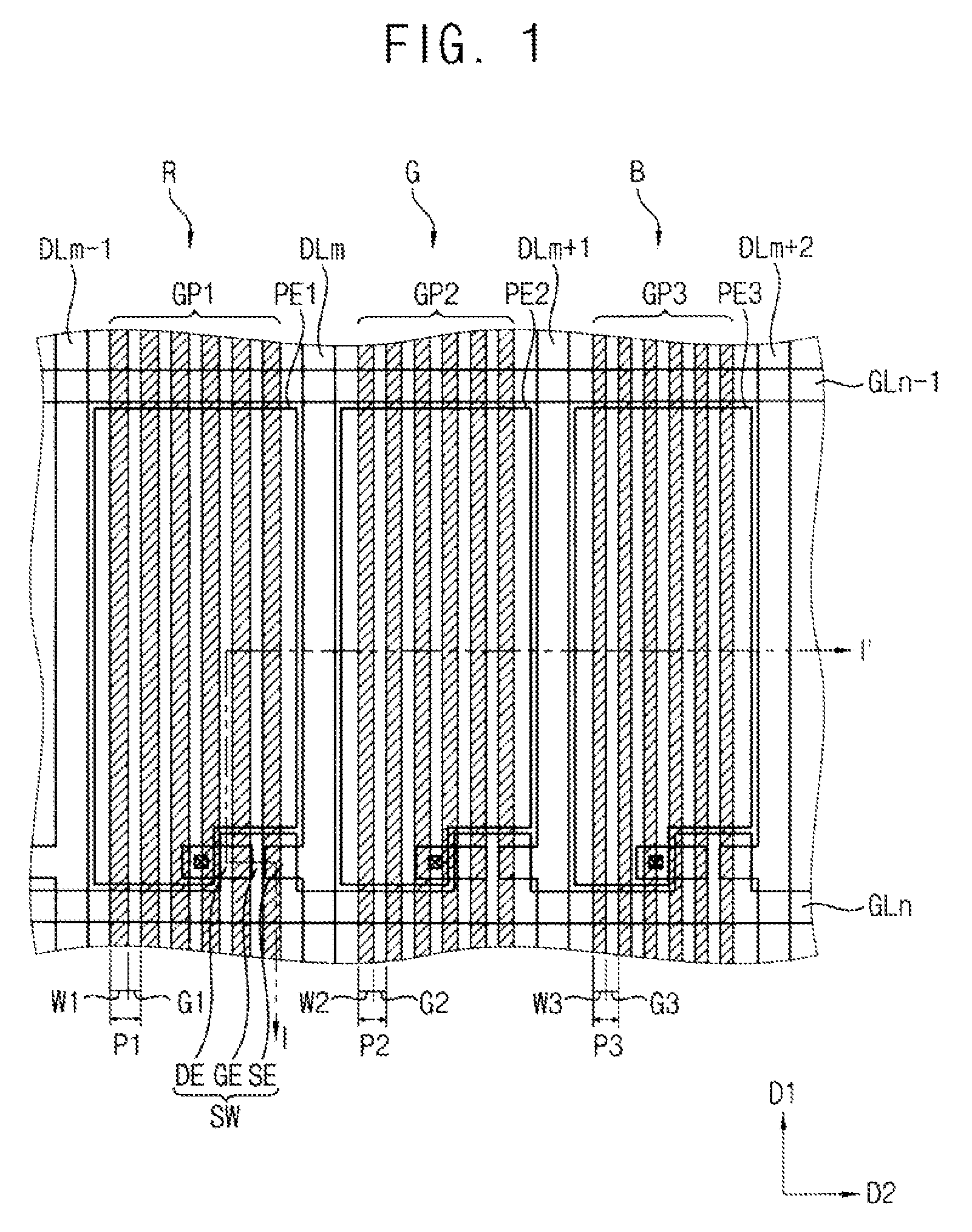
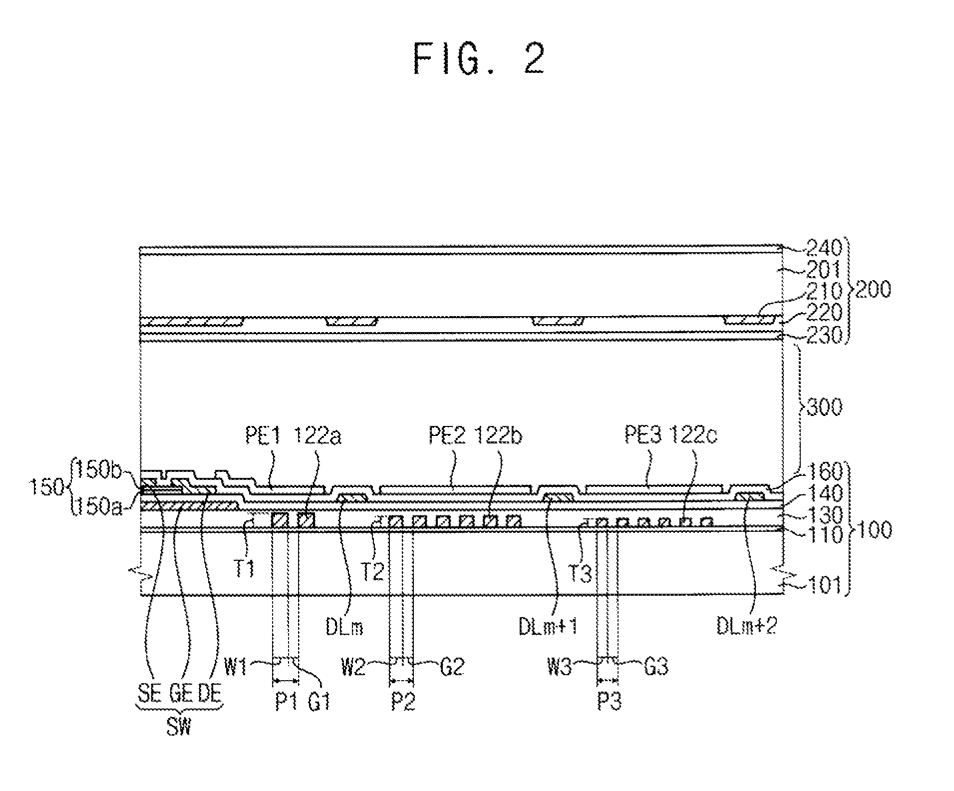
[0059]FIG. 1 is a plan view illustrating a display device in accordance with Exemplary Embodiment 1 of the present invention. FIG. 2 is a cross-sectional view taken along I-I′ in FIG. 1.

[0060]Referring to FIGS. 1 and 2, a display device in accordance with Exemplary Embodiment 1 of the present invention includes a first display substrate 100, a second display substrate 200 facing the first display substrate 100, and a liquid crystal layer 300 interposed between the first display substrate 100 and the second display substrate 200.

[0061]The first display substrate 100 includes a first base substrate 101. The first base substrate 101 may include glass. The first base substrate 101 includes a first color pixel region R, a second color pixel region G, and a third color pixel region B. The pixel regions may be adjacently arranged.

[0062]A first dielectric layer 110, a first lattice pattern GP1, a second lattice pattern GP2, a third lattice pattern GP3, and a second dielectric layer 130 may ...

exemplary embodiment 2

[0107]FIG. 7 is a cross-sectional view illustrating a display device in accordance with Exemplary Embodiment 2 of the present invention.

[0108]The display device described with reference to FIG. 7 may be substantially the same as the display device described with reference to FIG. 1 and FIG. 2 except that the first nano metal wires 124a, the second nano metal wires 124b and the third nano metal wires 124c have substantially the same thickness. Therefore, the same reference numbers are used for the same or similar elements, and any further descriptions concerning the same or similar elements as those shown in FIG. 1 and FIG. 2 will be omitted.

[0109]Referring to FIG. 7, a display device in accordance with Exemplary Embodiment 2 of the present invention includes a first display substrate 100a, a second display substrate 200 facing the first display substrate 100a, and a liquid crystal layer 300 interposed between the first display substrate 100a and the second display substrate 200.

[011...

exemplary embodiment 3

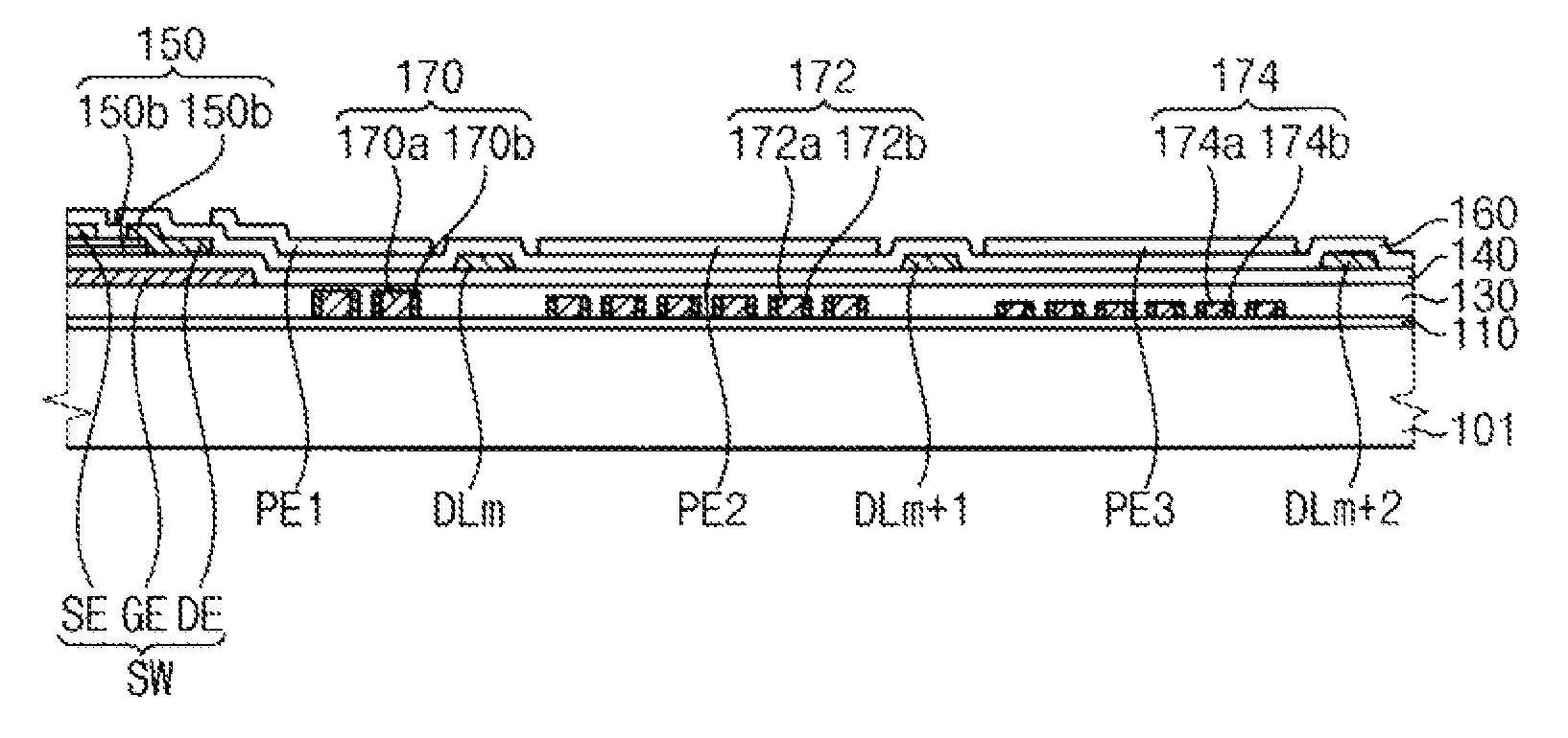
[0123]FIG. 9 is a cross-sectional view illustrating a display device in accordance with Exemplary Embodiment 3 of the present invention.

[0124]The display device described with reference to FIG. 9 may be substantially the same as the display device described with reference to FIG. 2 except first nano metal wires 170, second nano metal wires 172 and third nano metal wires 174. Therefore, the same reference numbers are used for the same or similar elements, and any further descriptions concerning the same or similar elements as those shown in FIG. 2 will be omitted.

[0125]Referring to FIG. 9, a display device in accordance with Exemplary Embodiment 3 of the present invention includes a first display substrate 100b, the second display substrate 200 facing the first display substrate 100b, and the liquid crystal layer 300 interposed between the first display substrate 100b and the second display substrate 200.

[0126]The first display substrate 100b may include a first base substrate 101, a...


PUM

PropertyMeasurementUnit
thickness T1aaaaaaaaaa
width W1aaaaaaaaaa
width W2aaaaaaaaaa

Abstract

A display substrate includes a base substrate, a first dielectric layer, a first lattice pattern, a second lattice pattern, and a second dielectric layer. The first lattice pattern is disposed on the first dielectric layer at a first color pixel region. The first lattice pattern includes a plurality of first nano metal wires. The second lattice pattern is disposed on the first dielectric layer at a second color pixel region. The second lattice pattern includes a plurality of second nano metal wires. The second nano metal wires have different dimensions from the first nano metal wires. The second dielectric layer covers the first nano metal wires and the second nano metal wires.

Description

PRIORITY STATEMENT[0001]This application claims priority under 35 U.S.C. §119 to Korean Patent Application No. 2009-0094488, filed on Oct. 6, 2009 in the Korean Intellectual Property Office (KIPO), the contents of which are herein incorporated by reference in their entirety.BACKGROUND OF THE INVENTION[0002]1. Field of the Invention[0003]The present invention relates to a display substrate, a method of manufacturing the display substrate, and a display device having the display substrate. More particularly, the present invention relates to a display substrate used in a liquid crystal display (LCD) device, a method of manufacturing the display substrate, and a display device having the display substrate.[0004]2. Description of the Related Art[0005]A liquid crystal display (LCD) device offers many desirable qualities such as thinness and light weight compared to a conventional cathode ray tube (CRT) display device, and is thus increasingly widely used. An LCD device includes an LCD pan...

Claims


Application Information

Patent Timeline
Patent Type & Authority Patents(United States)
IPC IPC(8): H01L29/20
CPCG02F1/133516G02F1/133528H01L27/1214G02F2001/133541G02F2203/10G02F1/133541H01L27/1218G02B5/30G02F1/1335
Inventor KIM, HYUN-WUKSHIN, SUNG-TAEKIM, KYEONG-HYEON
Owner SAMSUNG DISPLAY CO LTD
Why Eureka
Try Eureka