

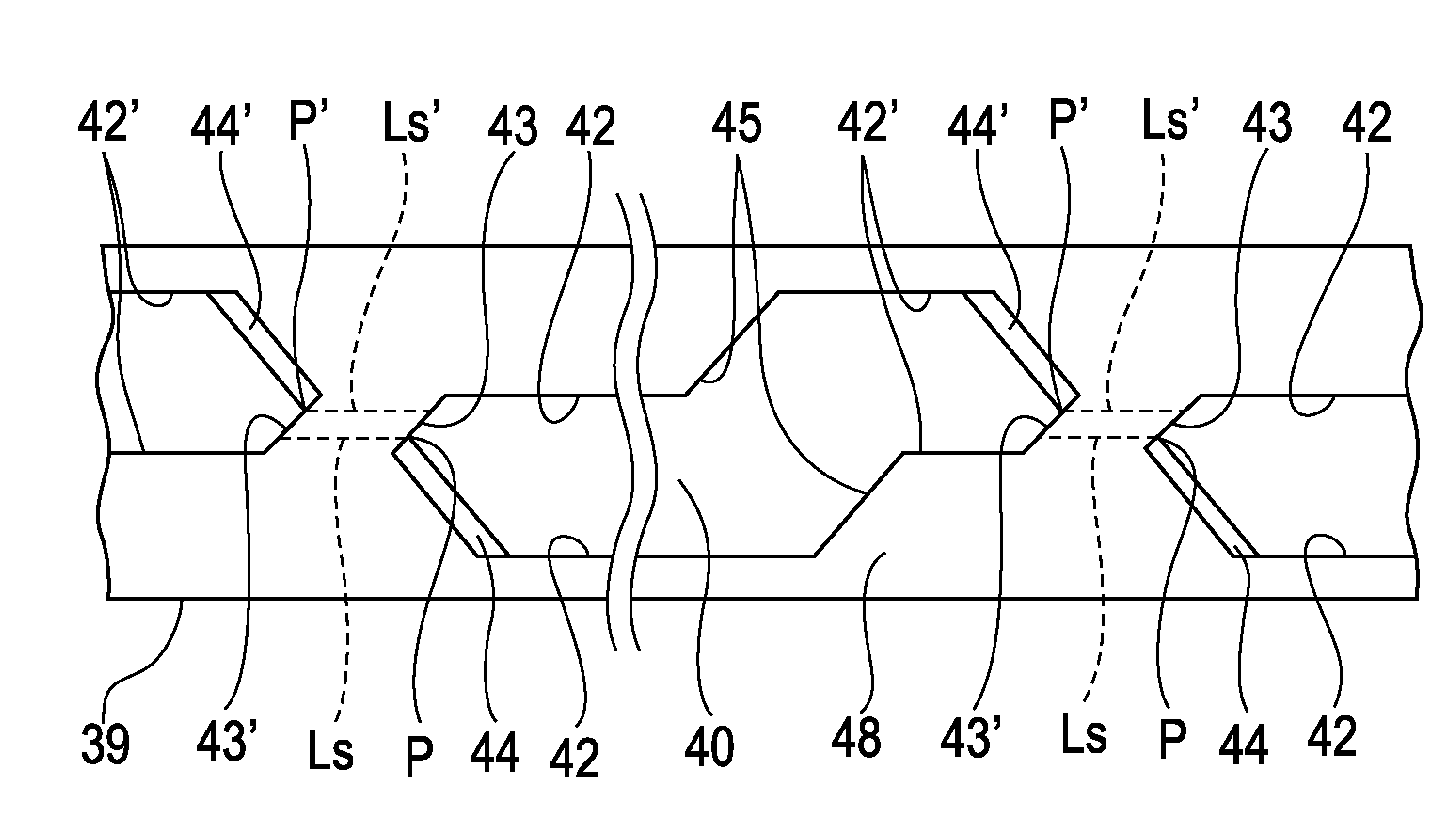
Break pattern of silicon wafer, silicon wafer, and silicon substrate
a technology of silicon wafers and substrates, applied in semiconductor devices, semiconductor/solid-state device details, printing, etc., can solve the problems of difficult to manage the shape of residual portions, inability to cut stably, and easy variation of size of residual portions, etc., to achieve the effect of cutting stably
- Summary
- Abstract
- Description
- Claims
- Application Information
AI Technical Summary
Benefits of technology
Problems solved by technology
Method used
Image

Examples
Embodiment Construction
[0026]Herein below, embodiments for carrying out the invention will be described with reference to the accompanying drawings. In addition, in the embodiments described below, there have been a variety limitation as preferred embodiment of the invention, but the scope of the invention is not limited thereto as long as there is no description of the effect that limits the invention in particular to these embodiments in the following description. In addition, as a liquid ejecting apparatus of the invention, an ink jet recording apparatus (hereinafter, referred to as a printer) is described as an example in the following.
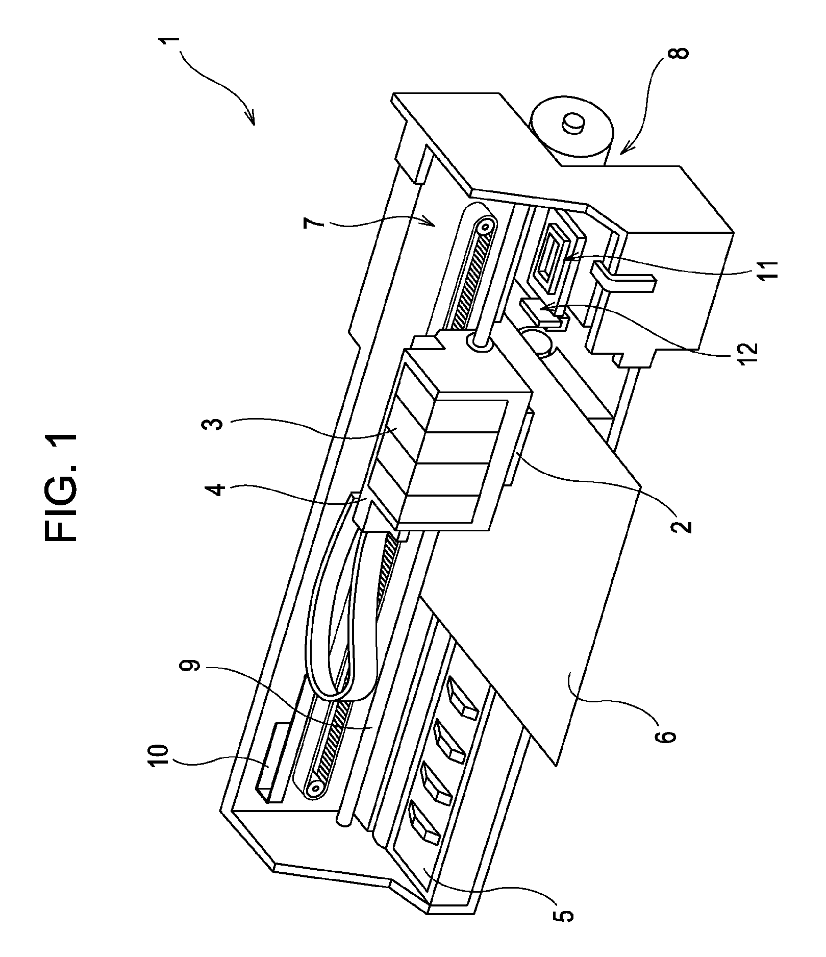
[0027]FIG. 1 shows a perspective view showing a configuration of a printer 1. This printer 1 is provided with a carriage 4 to which a recording head 2, which is a kind of liquid ejecting head, is attached and an ink cartridge 3, which is a kind of liquid supply source, is attached detachably, a platen 5 that is arranged below the recording head 2 when performing the rec...
PUM
 Abstract
Description
Claims
Application Information