Solid-state imaging apparatus and imaging system

a technology of solid-state imaging and imaging apparatus, which is applied in the field of solid-state imaging apparatus and imaging system, can solve problems such as limiting driving frequency, and achieve the effect of increasing the imaging area and reducing the influence of signal delay

Inactive Publication Date: 2013-08-13
CANON KK
View PDF95 Cites 15 Cited by
  • Summary
  • Abstract
  • Description
  • Claims
  • Application Information

AI Technical Summary

Benefits of technology

[0006]The present invention provides a solid-state imaging apparatus that is advantageous in reducing the influence of a signal delay caused by an increase in the imaging area.

Problems solved by technology

However, as the chip area increases, the problem of a signal delay caused by the parasitic resistance or the parasitic capacitance of signal lines surfaces, limiting the driving frequency.
However, Japanese Patent Laid-Open Nos. 2002-26302 and 2002-344809 do not consider this problem at all.

Method used


Image

  • Solid-state imaging apparatus and imaging system
  • Solid-state imaging apparatus and imaging system
  • Solid-state imaging apparatus and imaging system

Examples


Embodiment Construction

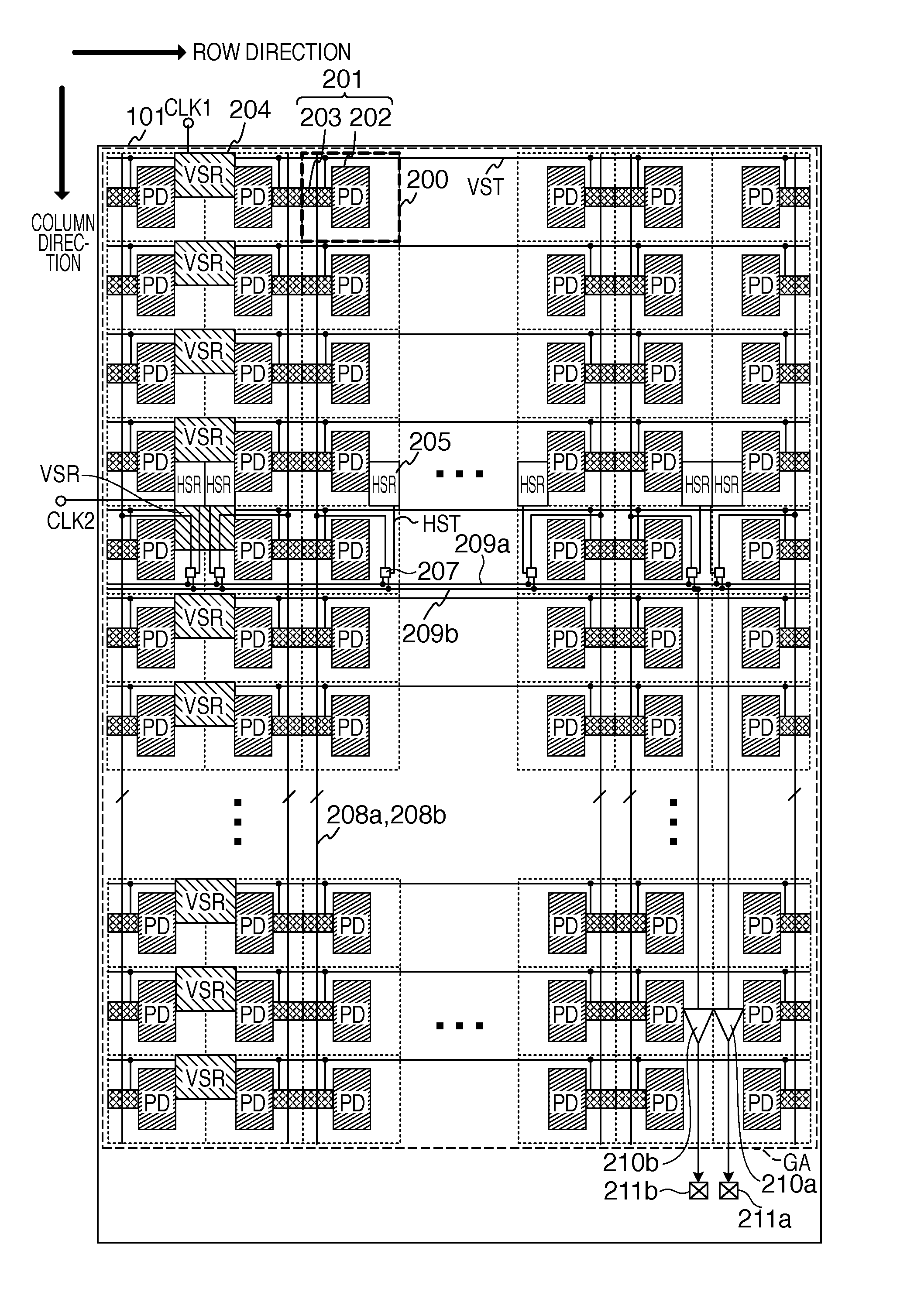
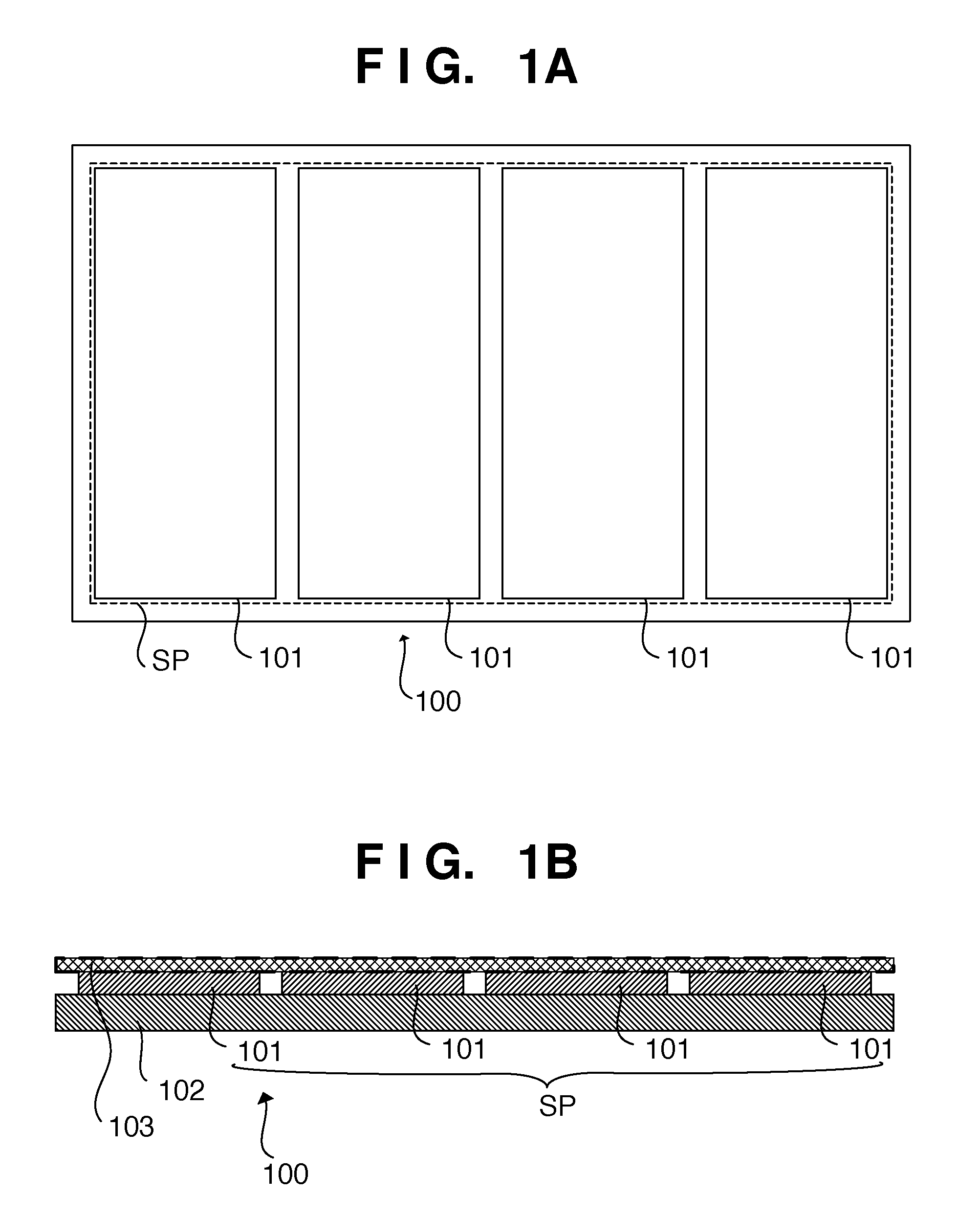
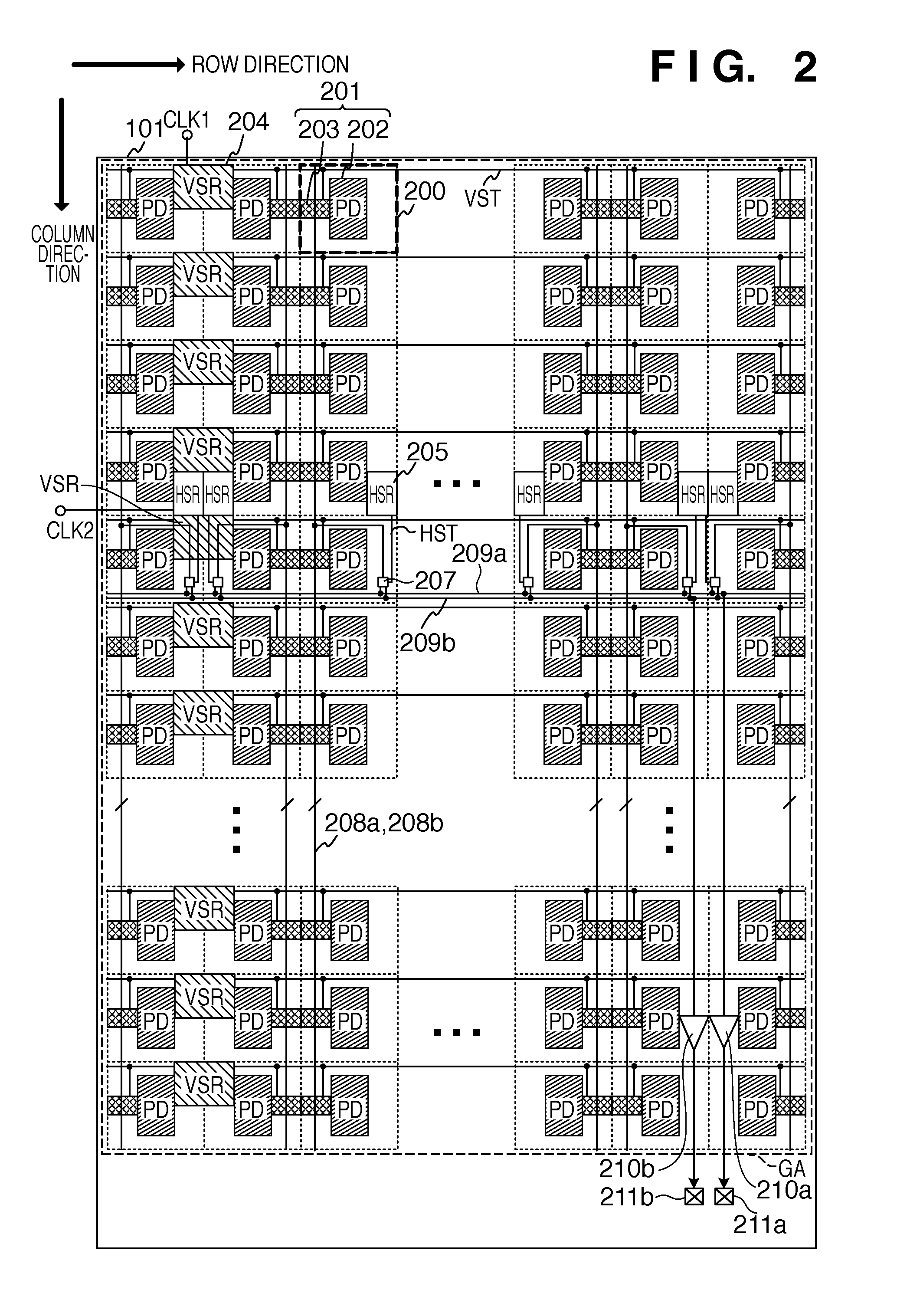
[0020]The schematic arrangement of a solid-state imaging apparatus 100 according to an embodiment of the present invention will be described with reference to FIGS. 1A and 1B. The solid-state imaging apparatus 100 can be formed by, for example, arraying a plurality of imaging blocks 101. In this case, an array of a plurality of imaging blocks 101 can form a sensor panel SP having one imaging region. The plurality of imaging blocks 101 can be arranged on a support substrate 102. When the solid-state imaging apparatus 100 uses a single imaging block 101, the single imaging block 101 forms the sensor panel SP. Each of the plurality of imaging blocks 101 may be provided by, for example, forming a circuit element on a semiconductor substrate or forming a semiconductor layer on, for example, a glass substrate and forming a circuit element on the semiconductor layer. Each of the plurality of imaging blocks 101 has a pixel array in which a plurality of pixels are arrayed so as to form plura...


PUM


Abstract

An imaging apparatus has an imaging area formed by arranging a plurality of imaging blocks each including a pixel array, a plurality of vertical signal lines, a horizontal output line commonly provided for the plurality of vertical signal lines to read out signals read out to the plurality of vertical signal lines, a first scanning circuit, and a second scanning circuit, wherein signals of the pixels of a selected row in the pixel array are read out to the plurality of vertical signal lines in accordance with a driving pulse from the first scanning circuit, the signals read out to the plurality of vertical signal lines are sequentially read out to the horizontal output line in accordance with a driving pulse from the second scanning circuit, and a length in a row direction of the pixel array is smaller than a length in a column direction of the pixel array.

Description

BACKGROUND OF THE INVENTION[0001]1. Field of the Invention[0002]The present invention relates to a solid-state imaging apparatus and an imaging system.[0003]2. Description of the Related Art[0004]Japanese Patent Laid-Open No. 2002-26302 discloses forming semiconductor circuits on rectangular semiconductor substrates in various sizes cut out from an ingot and combining the rectangular semiconductor substrates to manufacture a large-area radiation imaging apparatus. Japanese Patent Laid-Open No. 2002-344809 discloses coupling a plurality of image sensors and arranging a vertical shift register and a horizontal shift register in the effective area of each image sensor.[0005]When forming a large-area solid-state imaging apparatus by coupling a plurality of chips (corresponding to the rectangular semiconductor substrates with the semiconductor circuits in Japanese Patent Laid-Open No. 2002-26302 or the image sensors in patent reference 2), the area of each chip is preferably large. Howev...

Claims


Application Information

Patent Timeline
Patent Type & Authority Patents(United States)
IPC IPC(8): G01T1/24
CPCH04N5/32H04N5/3415H04N5/378H04N5/376H04N5/3745H04N25/41H04N25/616H04N25/74H04N25/771H04N25/77H04N25/75
Inventor ARISHIMA, YUYAMASHITA, YUICHIROFUJIMURA, MASARUKIKUCHI, SHINKONO, SHOJISHIMIZU, SHINICHIRO
Owner CANON KK
Why Eureka
Try Eureka