

Collaborative environment for physical verification of microdevice designs
a technology for physical verification and microdevices, applied in the field of collaborative environment for physical verification of microdevices, can solve the problems of increasing the difficulty of physical verification, affecting the quality of physical verification, so as to facilitate collaboration
- Summary
- Abstract
- Description
- Claims
- Application Information
AI Technical Summary
Benefits of technology
Problems solved by technology
Method used
Image

Examples
Embodiment Construction
Illustrative Operating Environment
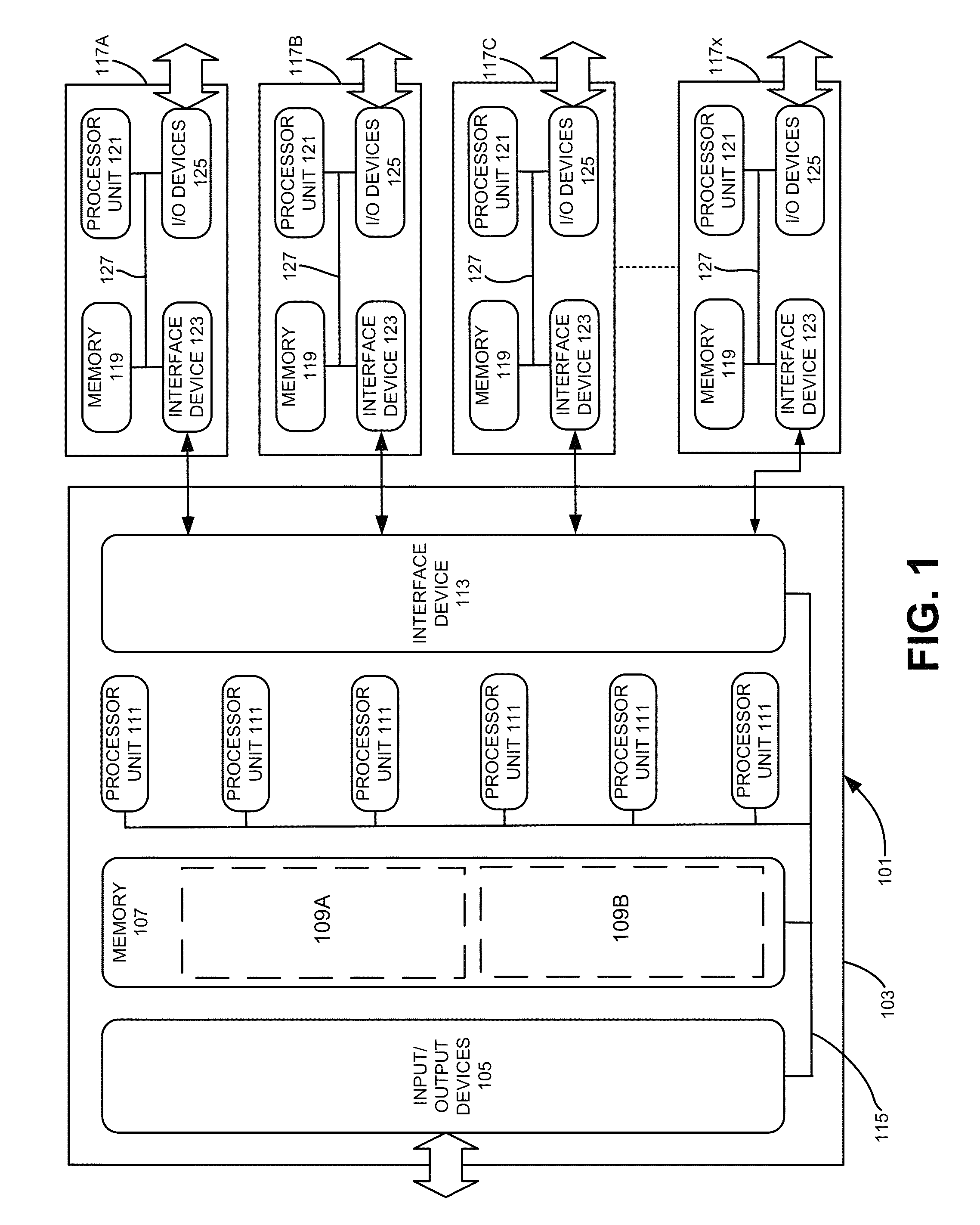
[0021]Various examples of a collaborative environment for one or more electronic design automation processes according to embodiments of the invention may be implemented by one or more programmable computing devices executing computer-executable software instructions. Alternately or additionally, various examples of a collaborative environment for one or more electronic design automation processes according to embodiments of the invention may be implemented by computer-executable software instructions stored in a computer-readable medium, such as a magnetic or optical storage device, or a solid state memory device. Because these embodiments of the invention may be implemented using software instructions, the components and operation of a generic programmable computer system through which various embodiments of the invention may be employed will first be described.
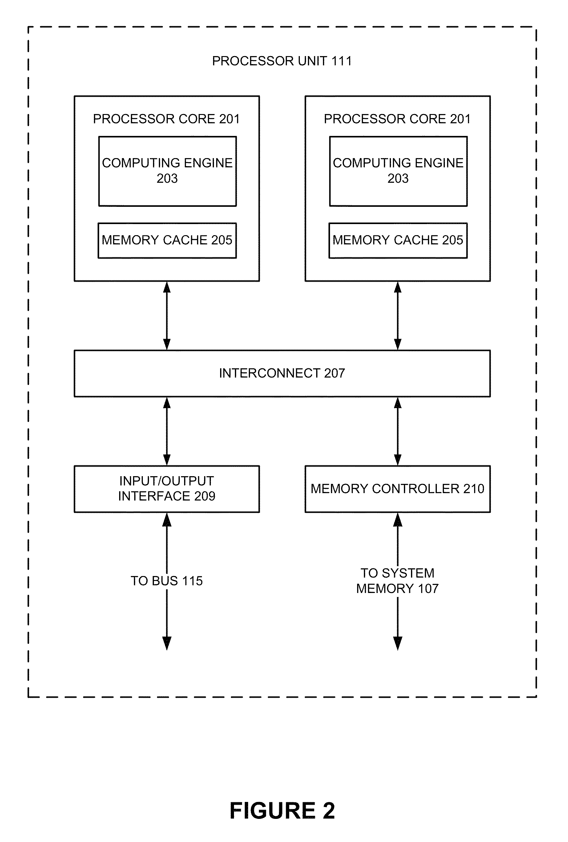
[0022]Further, because of the complexity of some electronic design automation processes...
PUM
 Abstract
Description
Claims
Application Information