
Vertical stacked light emitting structure

a light-emitting structure and vertical stack technology, applied in the direction of discharge tube luminescnet screens, discharge tube/lamp details, incadescent envelopes/vessels, etc., can solve the problems of high power consumption, high heat generation, and quick attenuation, and achieve the effect of increasing the light-emitting efficiency of instant disclosur

Inactive Publication Date: 2013-08-27
AZUREWAVE TEHNOLOGIES INC
View PDF4 Cites 9 Cited by
  • Summary
  • Abstract
  • Description
  • Claims
  • Application Information

AI Technical Summary

Benefits of technology

[0010]Therefore, because the at least one first LED bare chip, the at least one light guiding body, and the at least one second LED bare chip are stacked on top of one another sequentially, or the at least one first LED bare chip and the at least one second LED bare chip are stacked on top of one another sequentially, the light-emitting efficiency of the instant disclosure can be increased.

Problems solved by technology

Moreover, compared to the newly developed light-emitting-diode (LED) lamps, these traditional lamps have the disadvantages of quick attenuation, high power consumption, high heat generation, short service life, high fragility, and being not recyclable.
However, the LEDs only can be arranged along a horizontal direction, thus the usage number of the LEDs is limited in the limited horizontal space and the light emitting efficiency cannot be increased.

Method used


Image

  • Vertical stacked light emitting structure
  • Vertical stacked light emitting structure
  • Vertical stacked light emitting structure

Examples


first embodiment

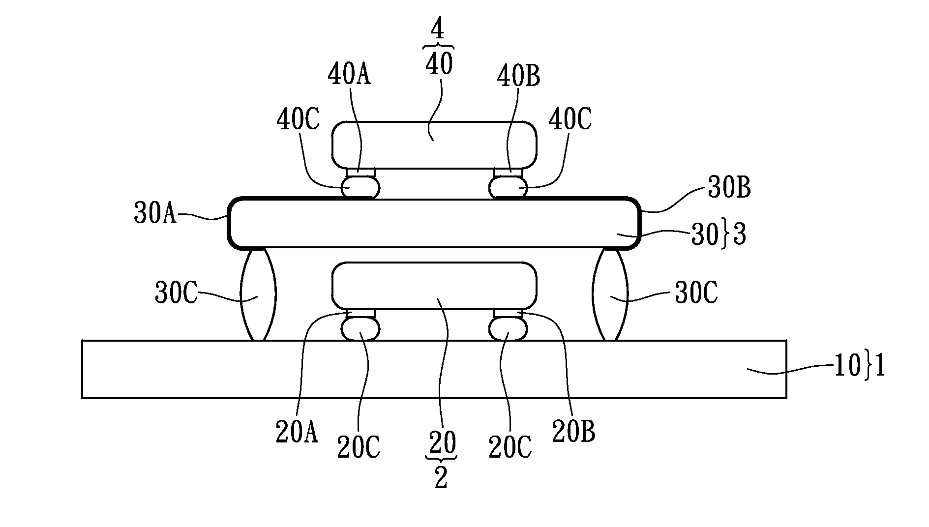
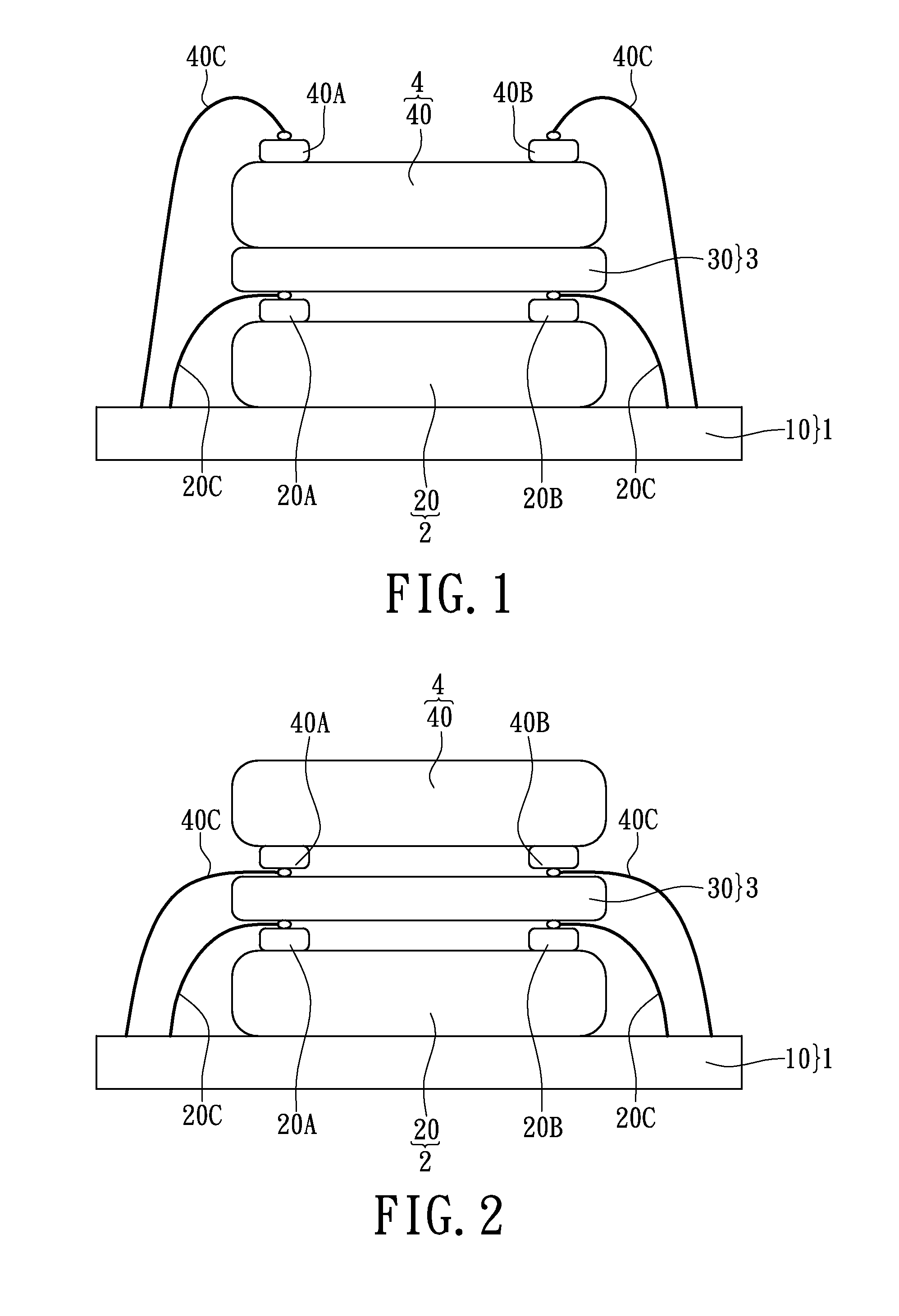
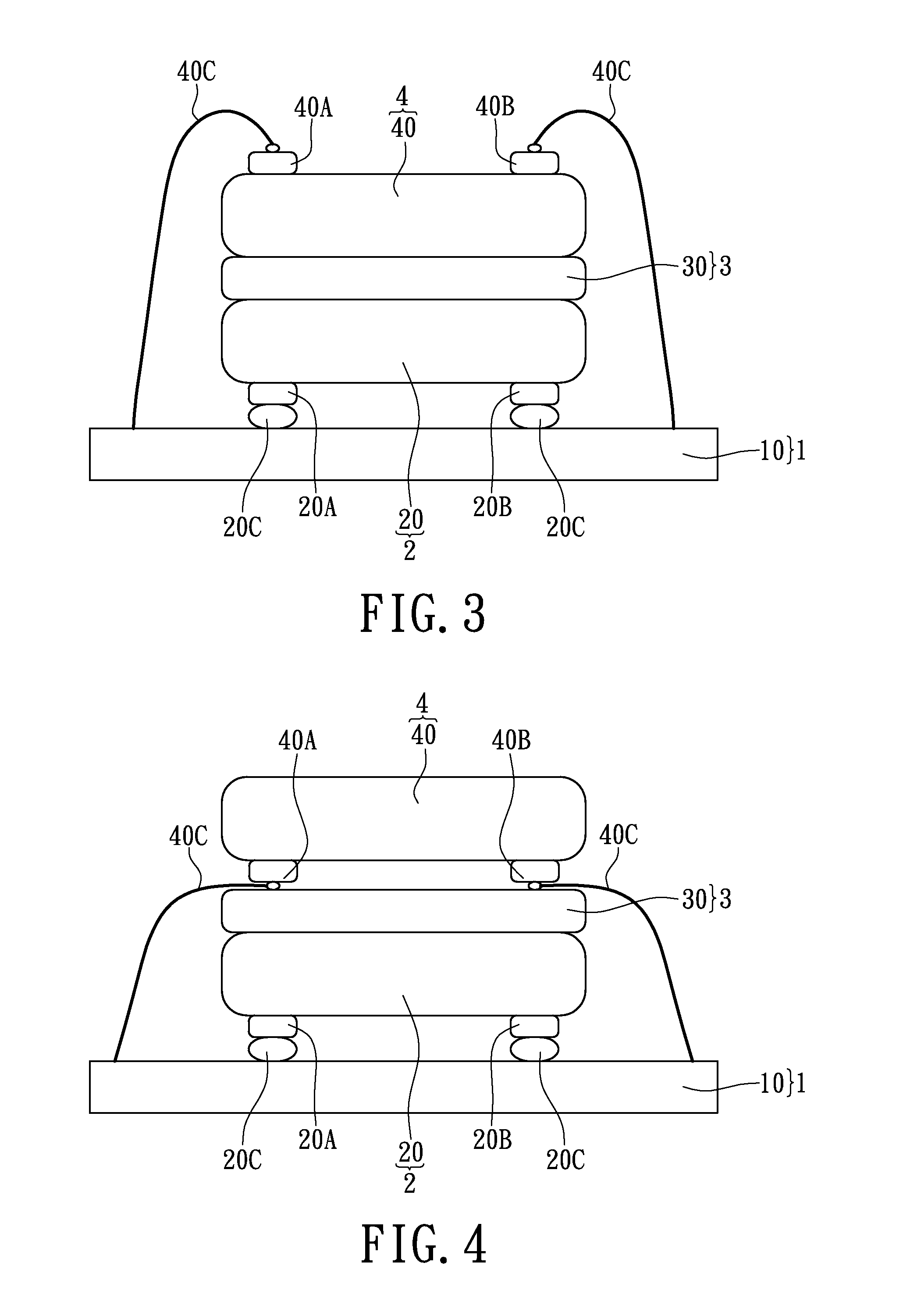
[0027]Referring to FIG. 1, where the first embodiment provides a vertical stacked light emitting structure, comprising: a substrate unit 1, a first light emitting unit 2, a light guiding unit 3, and a second light emitting unit 4. The first light emitting unit 2, the light guiding unit 3, and the second light emitting unit 4 are vertically and upwardly stacked on top of one another sequentially from the substrate unit 1.

[0028]The substrate unit 1 includes at least one substrate body 10. For example, the substrate body 10 may be a circuit substrate, and the circuit substrate has a plurality of conductive traces (not shown) disposed thereon.

[0029]Furthermore, the first light emitting unit 2 includes at least one first LED bare chip 20 disposed on the substrate body 10 and electrically connected to the substrate body 10. Of course, the instant disclosure can use a plurality of first LED bare chips 20 sequentially stacked on top of one another and electrically connected to the substrate...

second embodiment

[0032]Referring to FIG. 2, where the second embodiment provides a vertical stacked light emitting structure, comprising: a substrate unit 1, a first light emitting unit 2, a light guiding unit 3, and a second light emitting unit 4. In addition, the first light emitting unit 2 and the light guiding unit 3 are combined to form a stacked type light emitting module, and the second light emitting unit 4 is a flip-chip type light emitting module. Comparing FIG. 2 with FIG. 1, the difference between the second embodiment and the first embodiment is that: in the second embodiment, the second LED bare chip 40 has at least one second positive pad 40A and at least one second negative pad 40B disposed on the bottom surface thereof, the second positive pad 40A and the second negative pad 40B can simultaneously contact the top surface of the light guiding body 30, and at least two second conductive elements 40C (such as metal conductive wires) can be respectively electrically connected between th...

third embodiment

[0033]Referring to FIG. 3, where the third embodiment provides a vertical stacked light emitting structure, comprising: a substrate unit 1, a first light emitting unit 2, a light guiding unit 3, and a second light emitting unit 4. Comparing FIG. 3 with FIG. 1, the difference between the third embodiment and the first embodiment is that: in the third embodiment, the top surface of the first LED bare chip 20 can contact the bottom surface of the light guiding body 30, the first LED bare chip 20 has at least one first positive pad 20A and at least one first negative pad 20B disposed on the bottom surface thereof, and at least two first conductive elements 20C (such as solder balls) are respectively electrically connected between the first positive pad 20A and the substrate body 10 and between the first negative pad 20B and the substrate body 10. For example, the first positive pad 20A and the first negative pad 20B of the first LED bare chip 20 can be electrically connected to the subs...


PUM


Abstract

A vertical stacked light emitting structure includes a substrate unit, a stacked type light emitting module, and a flip-chip type light emitting module. The substrate unit includes a substrate body. The stacked type light emitting module includes a first light emitting unit and a light guiding unit. The first light emitting unit includes at least one first LED bare chip disposed on and electrically connected to the substrate body, and the light guiding unit includes at least one light guiding body disposed on the first LED bare chip. The flip-chip type light emitting module includes a second light emitting unit. The second light emitting unit includes at least one second LED bare chip disposed on the light guiding body and electrically connected to the substrate body. Hence, the first LED bare chip, the light guiding body, and the second LED bare chip are stacked on top of one another sequentially.

Description

BACKGROUND OF THE INVENTION[0001]1. Field of the Invention[0002]The instant disclosure relates to a light emitting structure, and more particularly, to a vertical stacked light emitting structure.[0003]2. Description of Related Art[0004]The invention of the lamp greatly changes the style of building construction and the lifestyle of human beings, allowing people to work during the night. Traditional lighting devices such as lamps that adopt incandescent bulbs, fluorescent bulbs, or power-saving bulbs have been generally well-developed and used intensively for indoor illumination.[0005]Moreover, compared to the newly developed light-emitting-diode (LED) lamps, these traditional lamps have the disadvantages of quick attenuation, high power consumption, high heat generation, short service life, high fragility, and being not recyclable. Thus, various high-powered LED structures are created to replace the traditional light sources. However, the LEDs only can be arranged along a horizonta...

Claims


Application Information

Patent Timeline
Patent Type & Authority Patents(United States)
IPC IPC(8): H01L33/00
CPCH01L25/0756H01L33/62H01L2224/16145H01L2224/48465
Inventor HSU, CHI-HSINGLU, CHUN-YUKUO, MING-CHE
Owner AZUREWAVE TEHNOLOGIES INC
Learn More