Light emitting diode (LED) lamp

a technology of light-emitting diodes and led lamps, which is applied in the direction of discharge tubes luminescnet screens, semiconductor devices for light sources, lighting and heating apparatus, etc., can solve the problems of difficult to ensure sufficient heat dissipation in leds, and achieve the effect of improving heat dissipation and limited size and shap

Active Publication Date: 2013-08-27
SAMSUNG ELECTRONICS CO LTD
View PDF10 Cites 6 Cited by
  • Summary
  • Abstract
  • Description
  • Claims
  • Application Information

AI Technical Summary

Benefits of technology

[0008]Provided is an LED lamp having improved heat dissipation by enlarging a heat dissipation area in a limited size and shape.

Problems solved by technology

When the supplied power is low, it is possible to realize sufficient heat dissipation in a LED having a limited size and shape, but, as the supplied power increases, it is difficult to assure sufficient heat dissipation in such a LED.

Method used


Image

  • Light emitting diode (LED) lamp
  • Light emitting diode (LED) lamp
  • Light emitting diode (LED) lamp

Examples


Embodiment Construction

[0035]Reference will now be made in detail to embodiments, examples of which are illustrated in the accompanying drawings. In the drawings, like reference numerals in the drawings denote like elements, and the size of each component may be exaggerated for clarity.

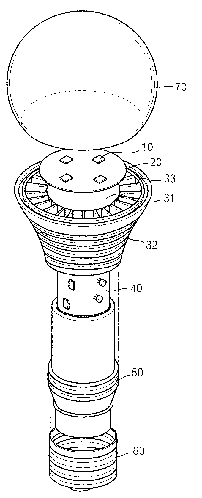
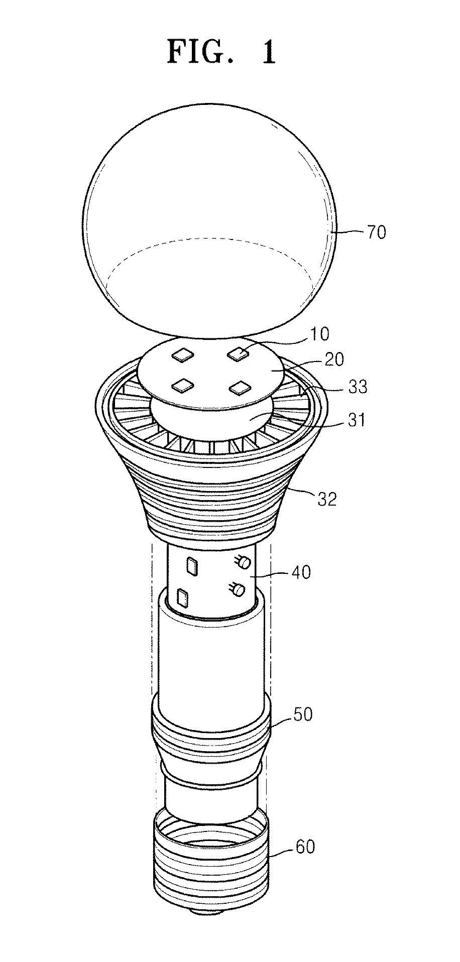
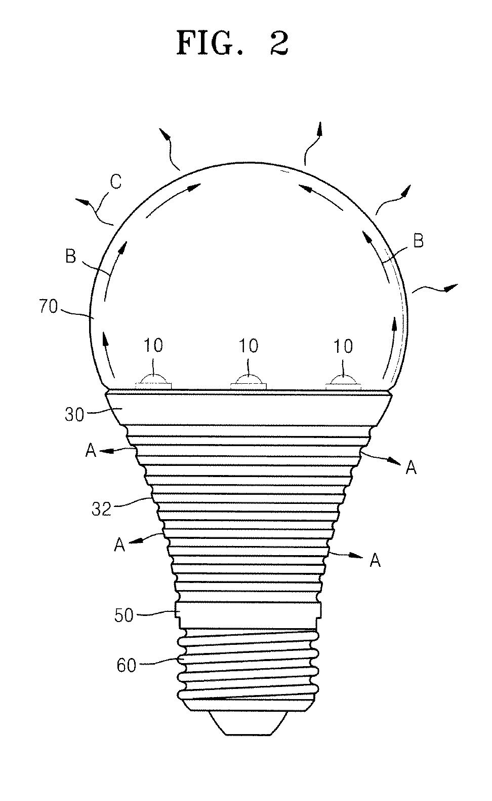
[0036]FIGS. 1 and 2 are diagrams respectively illustrating an exploded perspective view and a side view of a light emitting diode (LED) lamp according to an embodiment of the present invention. The LED lamp of FIGS. 1 and 2 satisfies the specification of an incandescent electric lamp.

[0037]Referring to FIGS. 1 and 2, an LED light-emitting device 10 is mounted on a circuit substrate 20. The LED light-emitting device 10 may be formed as an LED package obtained by packaging LED chips via a free mold method using a lead frame, a mold frame, a phosphor, and a light-transmitting filling material, and then may be mounted on the circuit substrate 20. Also, the LED light-emitting device 10 may be formed as an LED chip coated with ph...


PUM


Abstract

A light emitting diode (LED) lamp includes an emission unit comprising one or more LED light-emitting devices and a circuit substrate whereon the one or more LED light-emitting devices are mounted; a heat dissipating member whereon the emission unit is mounted and that dissipates heat generated by the emission unit; and a light-transmitting lamp cover directly contacting the heat dissipating member and coupled with the heat dissipating member so as to cover the emission unit, wherein the lamp cover is formed of a light-transmitting material having a thermal conductivity equal to or greater than 9 W / m·K−1.

Description

CROSS-REFERENCE TO RELATED APPLICATIONS[0001]This application claims the benefit of Korean Patent Application No. 10-2010-0120665, filed on Nov. 30, 2010, in the Korean Intellectual Property Office, the disclosure of which is incorporated herein in its entirety by reference.BACKGROUND[0002]1. Field[0003]The present disclosure relates to a light emitting diode (LED) lamp.[0004]2. Description of the Related Art[0005]Light emitting diodes (LEDs) are semiconductor devices capable of realizing light of various colors via a PN junction of a compound semiconductor. LEDs have a long lifetime, can be miniaturized, have light-weight, and can be driven at a low voltage due to their high directionality with respect to light. Also, since LEDs are highly resistant to shocks and vibrations, do not require a preheating time and complicated driving scheme, and can be packaged into various forms, they may be used in various applications.[0006]Recently, various attempts have been undertaken to replace...

Claims


Application Information

Patent Timeline
Patent Type & Authority Patents(United States)
IPC IPC(8): H01J1/02
CPCF21K9/00F21V3/04F21V17/12F21V17/164F21V29/86F21V29/713F21V29/004F21V5/007F21Y2103/003F21Y2105/001F21Y2101/02F21V29/506F21Y2103/10F21Y2105/10F21Y2115/10F21V29/70
Inventor YANG, HAENG-SEOKMOON, KI-HONGKANG, DAE-SUNGNA, YUN-WHANPARK, DAE-YEOP
Owner SAMSUNG ELECTRONICS CO LTD
Why Eureka
Try Eureka