
Capacitance extraction for advanced device technologies

a technology of advanced device technology and capacitor, applied in the direction of computer aided design, program control, instruments, etc., can solve the problem that the method does not have the speed or capacity to extract large-scale designs

Active Publication Date: 2013-08-27
SYNOPSYS INC
View PDF8 Cites 5 Cited by
  • Summary
  • Abstract
  • Description
  • Claims
  • Application Information

AI Technical Summary

Benefits of technology

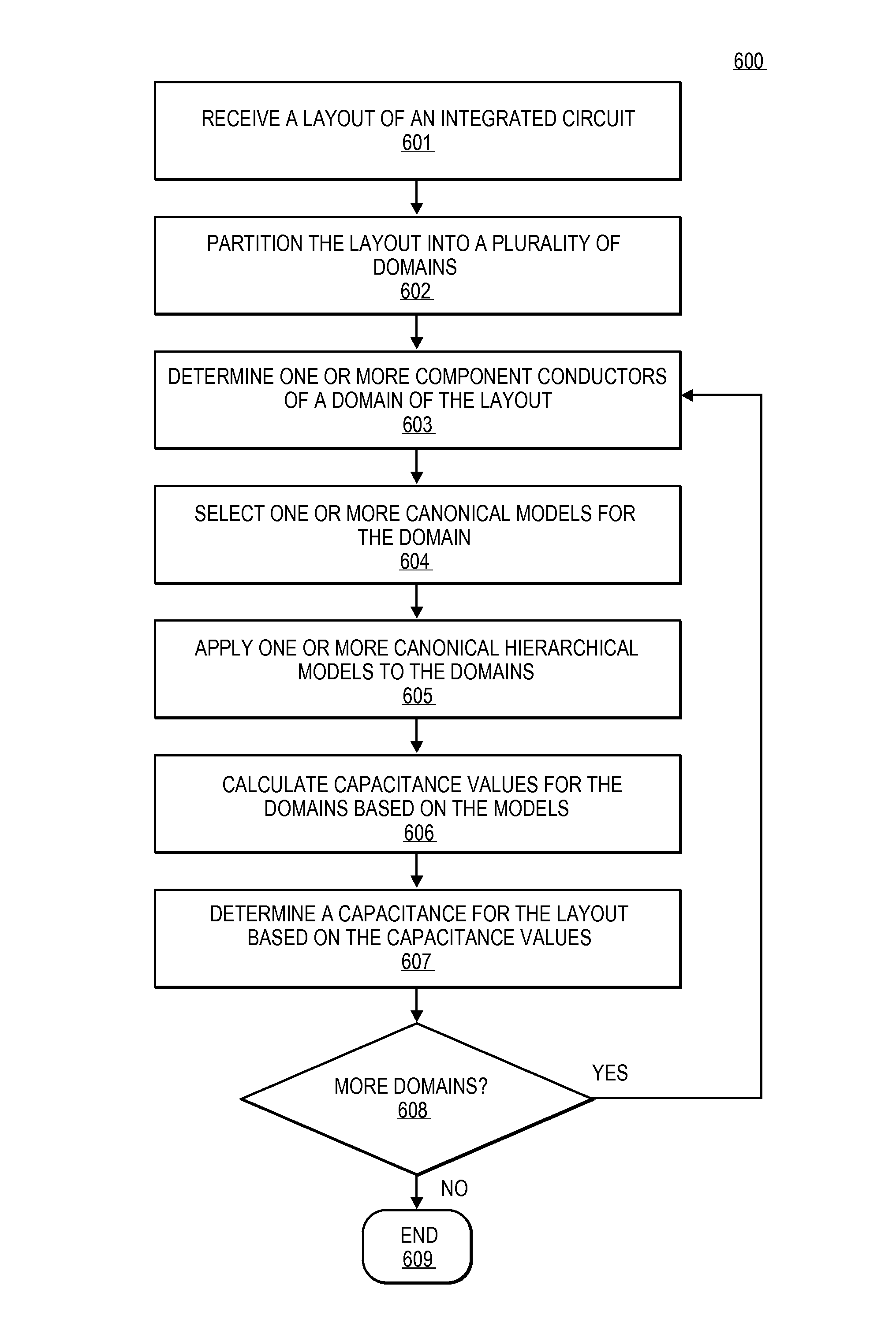
The patent describes methods and tools to extract capacitance for integrated circuits, particularly those with advanced device technologies. The methods involve creating models that capture the capacitance of devices with multiple conductors and between devices and other conductors. These models are applied to the layout of the integrated circuit to determine the overall capacitance. The patent provides a system to accurately analyze and mitigate potential issues in the circuit design, resulting in better performance and efficiency.

Problems solved by technology

Current process technologies that include the aforementioned advanced process features have several challenging characteristics for capacitance extraction.
These conducting layers are in close proximity and have unique physical characteristics that provide a challenge for capacitance extraction of a large-scale integrated circuit design.
These methods, however, do not have sufficient speed or capacity for extracting large-scale designs.

Method used


Image

  • Capacitance extraction for advanced device technologies
  • Capacitance extraction for advanced device technologies
  • Capacitance extraction for advanced device technologies

Examples


Embodiment Construction

[0030]The following description and drawings are illustrative and are not to be construed as limiting. Numerous specific details are described to provide a thorough understanding of embodiments as described herein. However, in certain instances, well known or conventional details are not described in order to avoid obscuring the description. References to an embodiment or one embodiment in the present disclosure are not necessary to the same embodiment; and, such references mean at least one.

[0031]Methods and apparatuses as described herein provide hierarchical modeling methodology for capacitance extraction of advanced devices. Hierarchical two dimensional (2D) / three dimensional (3D) models are constructed to accurately and efficiently capture complex device interactions for a capacitance extraction for an integrated circuit design.

[0032]At least some embodiments provide an accurate and efficient transistor-level capacitance extraction methodology for advanced device technologies i...


PUM


Abstract

A technology specific information to design the integrated circuit is received. A plurality of canonical hierarchical models to capture an integrated circuit capacitance are created. The plurality of canonical hierarchical models includes at least a canonical model to capture a capacitance of a device having a plurality of conductors, and a canonical model to capture a capacitance between at least a portion of the device and one or more other conductors of the integrated circuit. The canonical hierarchical models can be applied to a layout of the integrated circuit. A capacitance for the layout can be determined based on the canonical hierarchical models.

Description

FIELD[0001]Embodiments as described herein relate to designing of integrated circuits, and more particularly to capacitance extraction for an integrated circuit design.BACKGROUND[0002]For the design of integrated circuits (ICs) (e.g., on the scale of Very Large Scale Integration (VLSI) technology), designers often employ computer-aided techniques. Standard languages such as Hardware Description Languages (HDLs) have been developed to describe digital circuits to aid in the design and simulation of complex digital circuits. Generally, hardware description languages, e.g., VHDL and Verilog allow definition of a hardware model at a gate level, a register transfer level (RTL) or a behavioral level using abstract data types. As device technology continues to advance, various product design tools have been developed to adapt HDLs for use with newer devices and design styles.[0003]Typically, in designing an integrated circuit with an HDL code, the code is first written and then compiled by...

Claims


Application Information

Patent Timeline
Patent Type & Authority Patents(United States)
IPC IPC(8): G06F17/50
CPCG06F17/5081G06F17/5036G06F30/367G06F30/398
Inventor NIEUWOUDT, ARTHURKIM, JIYOUNKOSHY, MATHEWBISWAS, BARIBRATA
Owner SYNOPSYS INC
Learn More