Ceramic substrate material, method for the production and use thereof, and antenna or antenna array

a substrate material and ceramic technology, applied in the direction of printed circuit dielectrics, porous dielectrics, decorative arts, etc., can solve the problems of disadvantageous low resistance to moisture absorption of polyimides, unsatisfactory variations in the emission characteristic of substrates, etc., to achieve easy and cost-effective production, simple method, and reliable

Active Publication Date: 2013-09-10
MICRO SYST ENG
View PDF46 Cites 0 Cited by
  • Summary
  • Abstract
  • Description
  • Claims
  • Application Information

AI Technical Summary

Benefits of technology

[0011]The present invention allows a simple, cost-effective, and reliable method for the production of a ceramic substrate material which allows the configuration of thin-film structures on the porous areas. The invention also relates to a corresponding ceramic substrate material which allows the use of LTCC technology, and the implementation of components for ultra-high-frequency applications and / or further applications which require thin-film structures. In addition, the invention relates to suitable uses of a ceramic subject material of this type, including an antenna or an antenna array having a thick substrate material, which is producible easily and cost-effectively.

Problems solved by technology

Furthermore, the dielectric constant would change its is value depending on the degree of moisture, which would result in undesired variations in the emission characteristic of the substrate, and the device made therefrom (e.g., a radar sensor).
However, polyimides' low resistance to moisture absorption is disadvantageous.

Method used


Image

  • Ceramic substrate material, method for the production and use thereof, and antenna or antenna array
  • Ceramic substrate material, method for the production and use thereof, and antenna or antenna array
  • Ceramic substrate material, method for the production and use thereof, and antenna or antenna array

Examples


Embodiment Construction

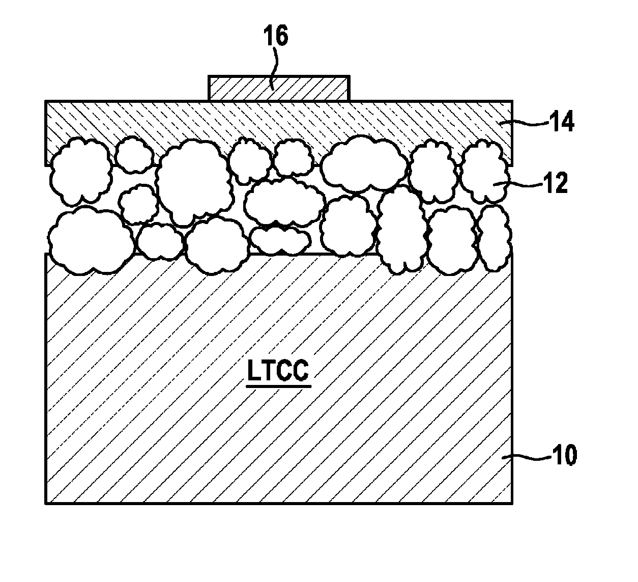
[0039]FIG. 2 shows (in section) a substrate material having a first layer 10 made of sintered glass ceramic, e.g., an LTCC tape having one of the following compositions:[0040]the composition 30% SiO2, 40% Al2O3, 4% CaO, 9% PbO, 2% B2O3+remainder—product identification DP951;[0041]the composition 30% SiO2, 20% Al2O3, 3% CaO, 5% SrO, 17% BaO, 5% ZnO+remainder—known as “Heraeus tape”, or[0042]the composition approximately 50% Al2O3, approximately 15% B2O3, approximately 15% La2O3+remainder−product identification DP943 from Hereaus.

[0043]The LTCC tape is laid in a suitable etching solution (e.g., phosphoric acid for DP951, Hereaus tape, and DP943) for porosification at a temperature of 110° C. The porosification procedure may alternatively also be performed using KOH (potassium hydroxide solution) of a concentration of approximately 40% at a temperature in the range of 80° C.

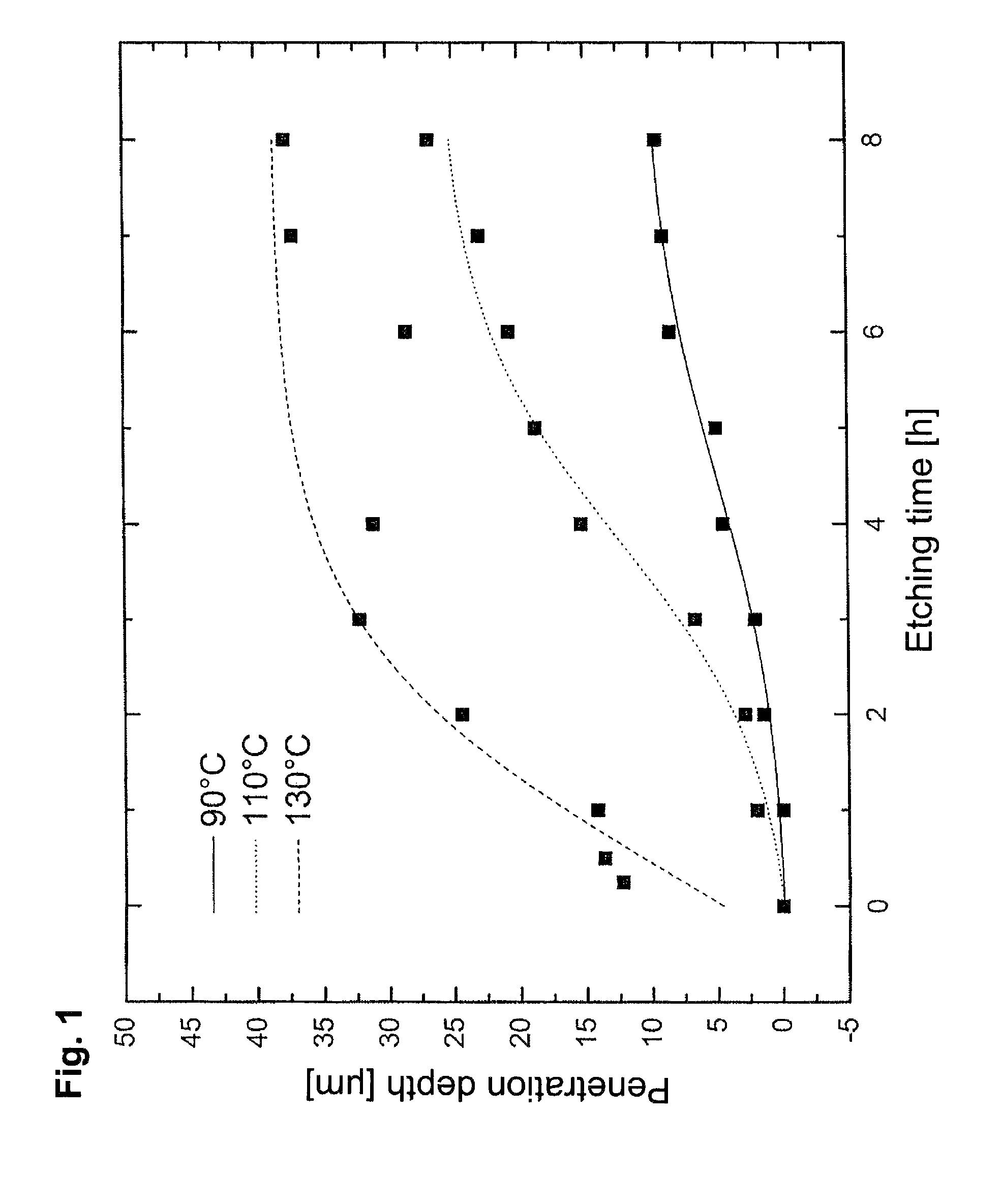
[0044]The curve shown in the diagram of FIG. 1 shows the dependence of the penetration depth of the etching solut...


PUM

PropertyMeasurementUnit
thicknessaaaaaaaaaa
thicknessaaaaaaaaaa
thicknessaaaaaaaaaa

Abstract

The invention relates to a ceramic substrate material having a first layer having a cavity structure formed therein, and at least one sealing layer situated on at least a part of the cavity structure. The first layer comprises at least one first component made of a crystalline ceramic material and/or a glass material as a matrix, the first layer containing a second component made of a further crystalline ceramic material, with selected mantle areas of the crystals and/or crystal agglomerates of the second component being etched out in such a way that the cavity structure is provided (preferably in the form of a pore and/or tube structure). The sealing layer seals the surface of the first layer in the areas on which it is situated (e.g., above the cavity structure), allowing application of thin-film structures to the cavity structure.

Description

FIELD OF THE INVENTION[0001]The invention relates to a ceramic substrate material having a first layer with a cavity structure, and a second layer applied as a seal above the cavity structure. The first layer includes at least one first component defining a matrix and being made of a crystalline ceramic material and / or a glass material, and a second component made of a further crystalline ceramic material. Mantle areas of the crystals and / or crystal agglomerates of the second component are at least regionally etched out to form the cavity structure, preferably in the form of a pore and / or tube structure. In addition, the present invention relates to the use of a ceramic substrate material of this type, and an antenna or an antenna array made of such material. Furthermore, the invention relates to a method for producing a ceramic substrate material of this type.BACKGROUND OF THE INVENTION[0002]Single-layer or multilayered ceramic substrate materials form important starting materials ...

Claims


Application Information

Patent Timeline
Patent Type & Authority Patents(United States)
IPC IPC(8): B31D3/00
CPCC03C17/28H01Q1/38H05K1/024C04B41/52C03C15/00C03C17/34C03C17/02H05K1/0306C04B41/009C04B41/89C03C17/38C04B41/4582C04B41/5023C04B41/5353C04B41/4539C04B41/5022C04B41/4537C04B41/522C04B41/488C04B35/00Y10T428/24562H05K2203/1147C04B2111/00844C03C2218/116C03C2218/119H05K2201/0195H05K2201/0116C03C2218/31C03C2218/113
Inventor SCHWANKE, DIETERHARNACK, MIRCOBITTNER, ACHIMSCHMID, ULRICH
Owner MICRO SYST ENG
Why Eureka
Try Eureka