Method and device for determining ionizing radiation

a technology of ionizing radiation and ionizing radiation, which is applied in the direction of individual semiconductor device testing, measurement with semiconductor devices, instruments, etc., can solve the problems of high detector cost, bulky badge form for personal dosimetry, and ineffective sense of ionizing radiation

Inactive Publication Date: 2013-09-17
INDIAN INSTITUTE OF TECHNOLOGY BOMBAY
View PDF9 Cites 0 Cited by
  • Summary
  • Abstract
  • Description
  • Claims
  • Application Information

AI Technical Summary

Benefits of technology

[0009]Another object of the invention is to provide a method for determining ionizing radiation which method is simple and easy to carry out, versatile and is cost effective.
[0010]Another object of the invention is to provide an electronic device for determining ionizing radiation which device is simple in construction and operation and is cost effective.
[0012]Another object of the invention is to provide an electronic device for determining ionizing radiation which device has additional advantages like large area coverage and structural flexibility.

Problems solved by technology

As a result, at higher temperatures, the effect of ionizing radiation is not as effectively sensed as at low temperatures.
The cost of the detector is also very high because of the inorganic silicon semiconductor technology being costly.
It is also bulky to realize in a badge form for personal dosimetry and expensive.
Immediate or real time read out is not possible with the TLD as it has to be heated to give the radiation dose output.
It may cause accidental or unintentional release of trapped electrons in the thermoluminescent material prior to read out by exposure to heat, or light, particularly ultraviolet, thereby creating measurement errors.
Humidity can also affect the working of the TLD and degrade efficiency thereof.

Method used


Image

  • Method and device for determining ionizing radiation
  • Method and device for determining ionizing radiation
  • Method and device for determining ionizing radiation

Examples


Embodiment Construction

[0016]According to the invention there is provided use of an organic semiconducting material sensor for determining ionizing radiation proportional to the change in resistivity or conductivity of the sensor.

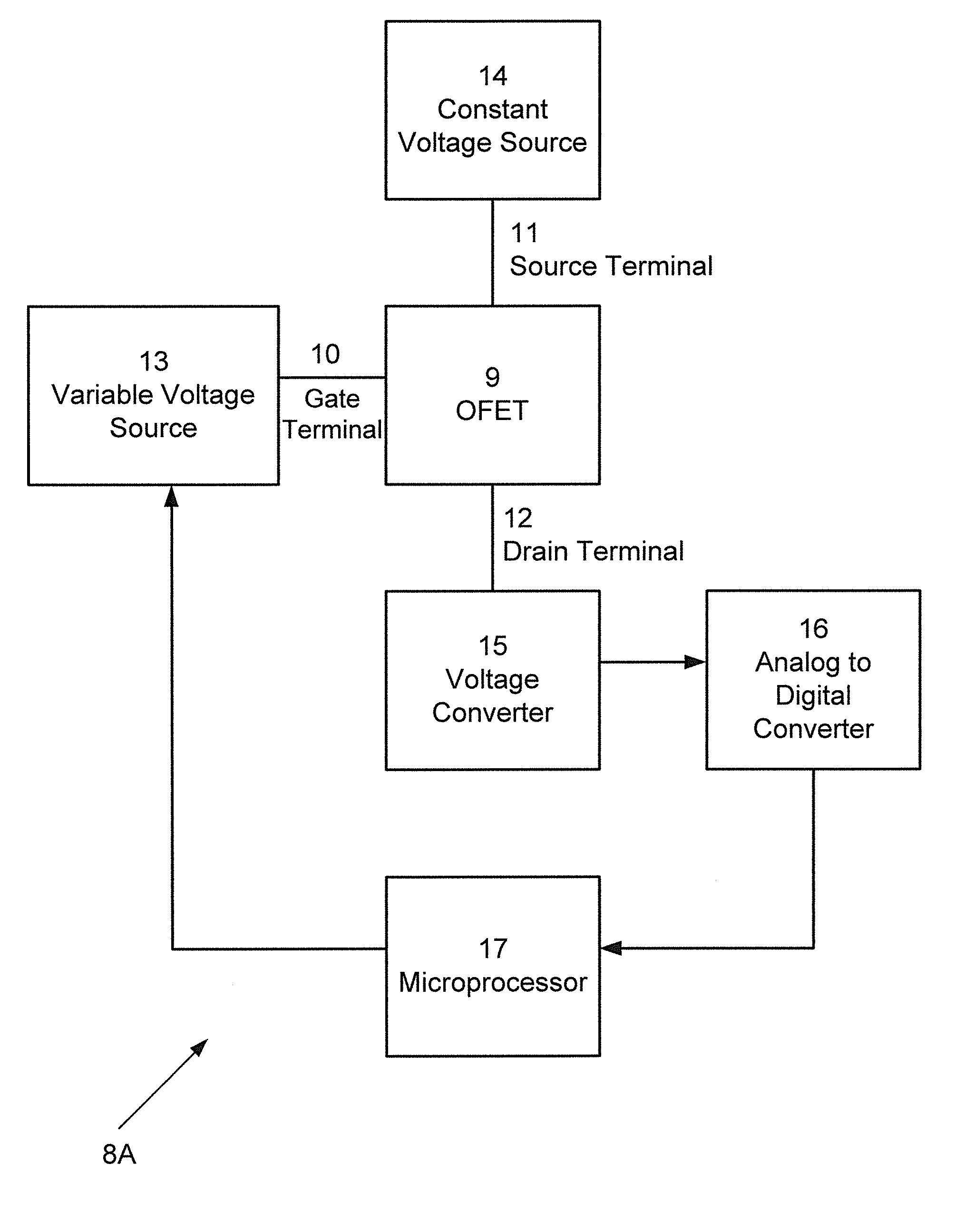
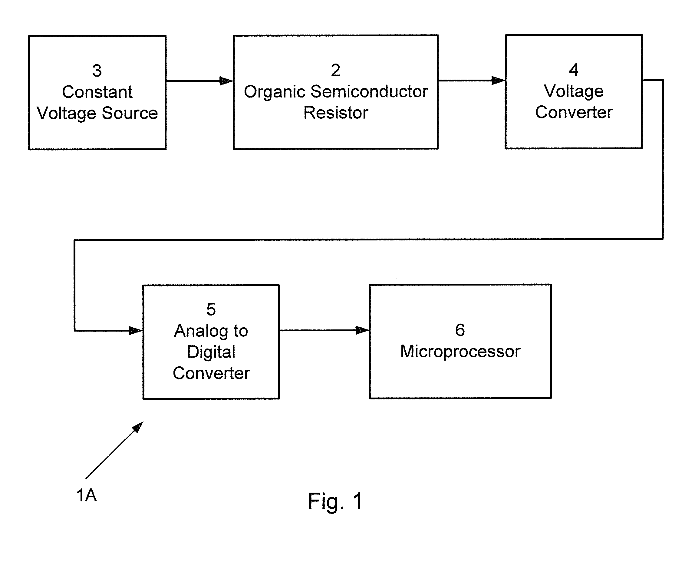
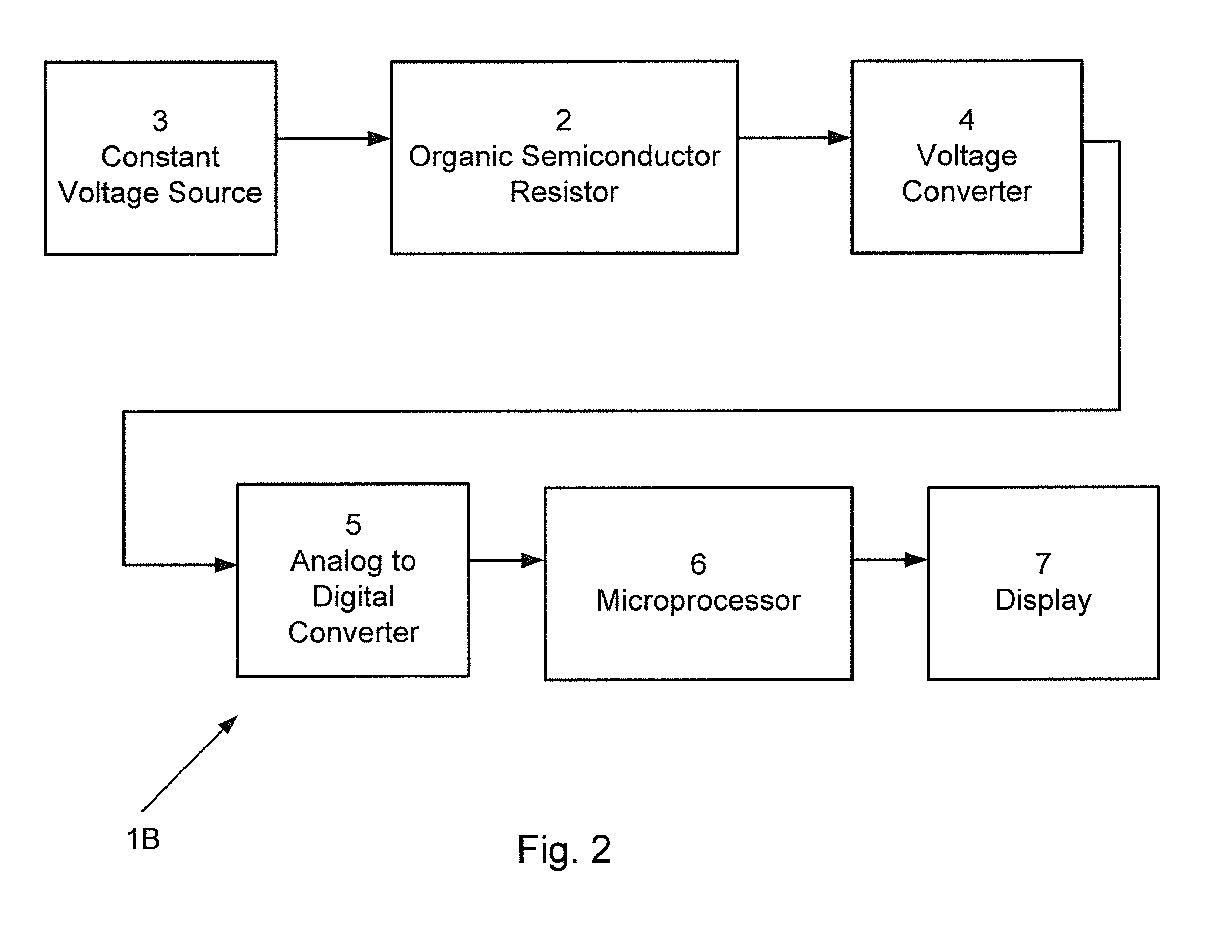
[0017]According to the invention there is also provided a method for determining ionizing radiation comprising the steps of:[0018](i) applying a constant voltage across an organic semiconducting material sensor prior to and after exposure of the sensor to the ionizing radiation;[0019](ii) measuring and converting the current passing through the sensor proportional to the conductivity or resistivity of the sensor which in turn is proportional to the ionizing radiation in the sensor, into a proportional analog voltage value; and if desired converting the analog voltage value into digital value; and[0020](iii) comparing the analog / digital values obtained prior to and after exposure of the sensor to the ionizing radiation and computing the ionizing radiation based on the change in th...


PUM


Abstract

A method for determining ionizing radiation including applying a constant voltage across an organic semiconducting material sensor prior to and after exposure of the sensor to the ionizing radiation; measuring and converting the current passing through the sensor proportional to the conductivity or resistivity of the sensor which in turn is proportional to the ionizing radiation in the sensor, into a proportional analog voltage value; and comparing the value obtained prior to and after exposure of the sensor to the ionizing radiation and computing the ionizing radiation based on the change in the value. An electronic device for determining ionizing radiation including an organic semiconductor resistor, a constant voltage source, and to a current to voltage converter, an analog to digital converter, and a microprocessor.

Description

FIELD OF THE INVENTION[0001]This invention relates to a method and device for determining ionizing radiation.BACKGROUND OF THE INVENTION[0002]Operational performance of electronic devices are reported to degrade with their exposure to ionizing radiation (Andrew Holmes-Siedle and Leonard Adams. “The Development of an MOS Dosimeter for use in Space”. IEEE Trans. Nucl. Sci., 25 (6), pp. 1607-1612, 1978; N. Bhat and J. Vasi, “Interface-state generation under radiation and high-field stressing in RNO MOS capacitors,” IEEE Trans. Nucl. Sci., 39, 2230, 1992.). Radiation effects are a matter of grave concern for space environment, nuclear applications and electronic gadgets operating in radiation prone environment. These radiation effects can be used in the positive sense as application of these devices in radiation dosimetry. (L. J. Asensio et. al., “Evaluation of a low-cost commercial mosfet as radiation dosimeter”, Sensors and Actuators, A 125, pp. 288-295, 2006.). Use of PMOS transistor...

Claims


Application Information

Patent Timeline
Patent Type & Authority Patents(United States)
IPC IPC(8): G01R27/08G01R31/02G01T3/08
CPCG01T1/00G01T1/026H01L27/308G01T1/26H01L31/115H10K39/36
Inventor RAVAL, HARSHIL NARENDRATIWARI, SHREE PRAKASHNAVAN, RAMESH RAJURAO, RAMGOPAL VALIPEKUMAR, ANIL
Owner INDIAN INSTITUTE OF TECHNOLOGY BOMBAY
Why Eureka
Try Eureka