Bow-balanced 3D chip stacking

a 3d chip and stacking technology, applied in the direction of semiconductor devices, semiconductor/solid-state device details, electrical devices, etc., can solve the problems of difficult bonding even three wafers, non-uniform thickness of each substrate, and high cost and time consumption of processes, so as to achieve the effect of maximum cancellation of wafer bows

Inactive Publication Date: 2013-10-01
IBM CORP
View PDF9 Cites 48 Cited by
  • Summary
  • Abstract
  • Description
  • Claims
  • Application Information

AI Technical Summary

Benefits of technology

[0006]The present invention provides a method of vertically stacking multiple semiconductor substrates while maximally compensating the wafer bow in each of the semiconductor substrates. A first set of semiconductor substrates includes semiconductor chips having bonding pads arranged in a primary pattern. A second set of semiconductor substrates includes semiconductor chips having bonding pads arranged in a mirror-image pattern, which is the pattern of the mirror image of the primary pattern. A first semiconductor substrate from the first set is bonded to a second semiconductor substrate from the second set such that each bonding pad is bonded to a mirror-image bonding pad. Additional substrates are bonded sequentially such that the bonded structure includes an even number of semiconductor substrates of which one half have bonding pads of the primary pattern and are bonded to the side of the first semiconductor substrate, while the other half have bonding pads of the mirror-image pattern and are bonded to the side of the second semiconductor substrate. The mirror-image patterns of the bonding pads enable maximal cancellation of wafer bow to enable stacking of multiple semiconductor substrates by limiting the total wafer bow of the bonded structure.

Problems solved by technology

Limiting factors in the increase in the number of layers in a three-dimensional integration ODD stack include bowing of the substrates at wafer bonding and non-uniformity of thickness within each substrate.
Thus, bonding even three wafers can be a challenge with current 3D integration technology.
While it is possible in theory to minimize the bow introduced by top wafer processing in FEOL and BEOL processing steps and bonding process steps, for example, by employing film compensation techniques, such processes are costly and time consuming.
In practice, the change of wafer bow due to FEOL and BEOL processing steps and the bonding process steps is unavoidable due to process limitations.
Because the total bow of bonded structures is cumulative, even a small change of wafer bow can result in a significant wafer bow when multiple wafers stacked.

Method used


Image

  • Bow-balanced 3D chip stacking
  • Bow-balanced 3D chip stacking
  • Bow-balanced 3D chip stacking

Examples


Embodiment Construction

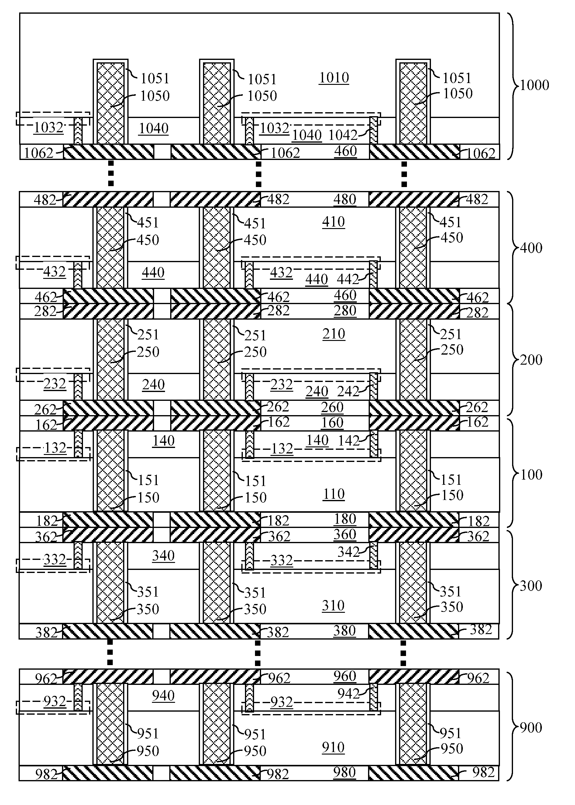
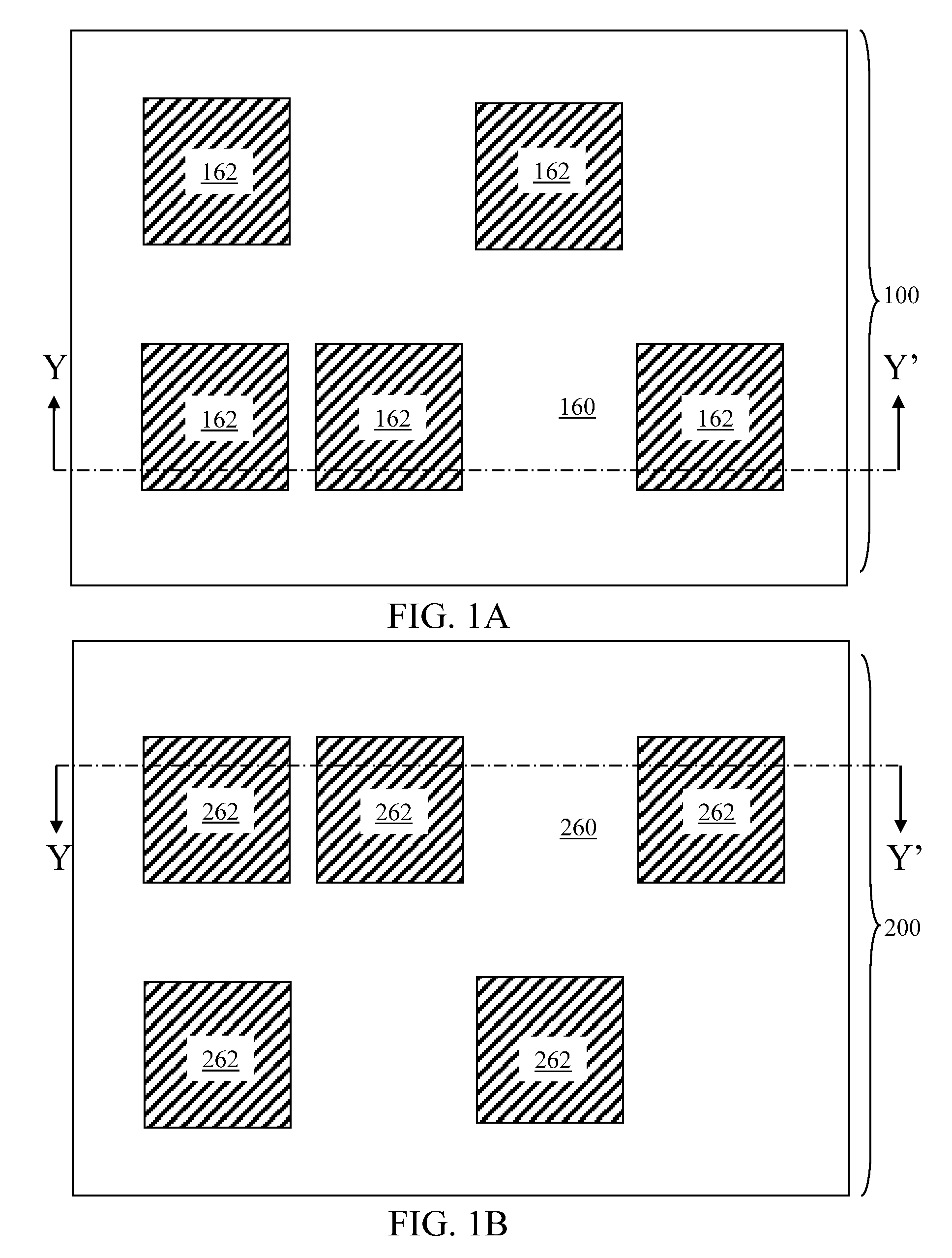
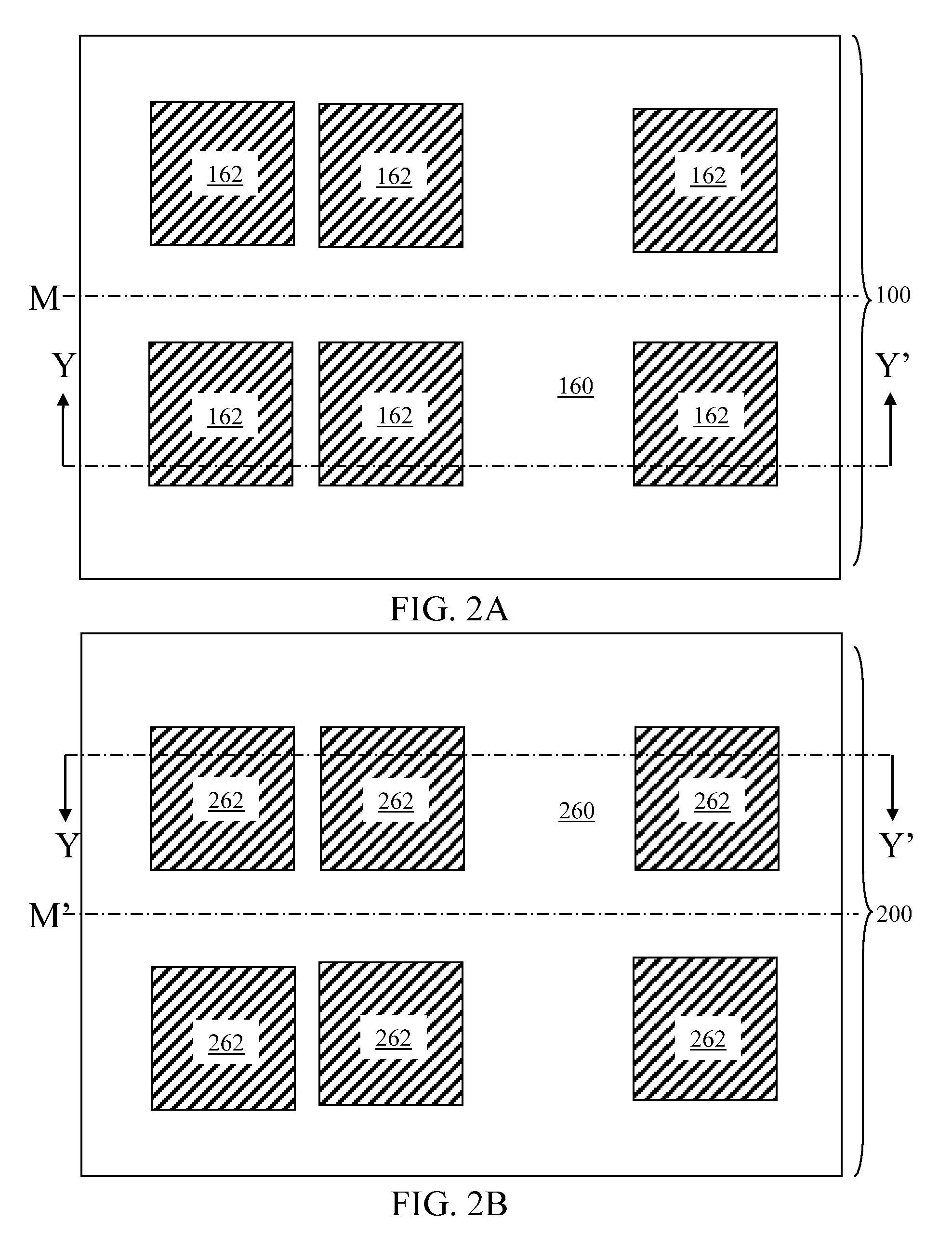
[0016]As stated above, the present invention relates to methods of stacking semiconductor substrates while maximally compensating for bowing of the semiconductor substrates and a bonded assembly of a plurality of substrates thereby formed, which are now described in detail with accompanying figures. Throughout the drawings, the same reference numerals or letters are used to designate like or equivalent elements. The drawings are not necessarily drawn to scale.

[0017]As used herein, a “semiconductor chip” is a structure including at least one of an integrated circuit, a passive component such as a capacitor, a resistor, an inductor, or a diode, or a micro-mechanical-electrical structure (MEMS), or a combination thereof that may be formed on a substrate including a semiconductor material.

[0018]As used herein, a “semiconductor substrate” refers to any substrate including a semiconductor material that is suitable for formation of semiconductor devices known in the art. A semiconductor su...


PUM


Abstract

A first set of semiconductor substrates includes semiconductor chips having bonding pads arranged in a primary pattern. A second set of semiconductor substrates includes semiconductor chips having bonding pads arranged in a mirror-image pattern. A first semiconductor substrate from the first set is bonded to a second semiconductor substrate from the second set such that each bonding pads is bonded to a mirror-image bonding pad. Additional substrates are bonded sequentially such that the bonded structure includes an even number of semiconductor substrates of which one half have bonding pads of the primary pattern and are bonded to the side of the first semiconductor substrate, while the other half have bonding pads of the mirror-image pattern and are bonded to the side of the second semiconductor substrate. The mirror-image patterns of the bonding pads enable maximal cancellation of wafer bow.

Description

BACKGROUND[0001]The present invention relates to methods of forming a semiconductor structure, and particularly to methods of stacking semiconductor substrates while maximally compensating for bowing of the semiconductor substrates and a bonded assembly of a plurality of substrates thereby formed.[0002]3D integration, or chip stacking, refers to a method of assembling two or more semiconductor chips so that the semiconductor chips that are placed in physical proximity to one another are also electrically connected among one another. 3D integration is typically performed vertically, i.e., one chip is placed above or below another chip. When two chips are brought together vertically, a set of conductive contact structures on the top surface of an underlying chip is aligned to another set of conductive contact structures on the bottom surface of an overlying chip. The conductive structures may be formed on the side of metal interconnect structures, or they may be formed on the side of ...

Claims


Application Information

Patent Timeline
Patent Type & Authority Patents(United States)
IPC IPC(8): H01L21/00H01L23/02
CPCH01L25/0657H01L25/50H01L24/05H01L2924/0002H01L2924/1305H01L2924/1461H01L2924/1301H01L2224/0401H01L2924/01327H01L2924/3511H01L2221/68359H01L2221/68363H01L2221/68377H01L2224/0557H01L2224/16145H01L2225/06541H01L2924/10252H01L2924/10253H01L2924/10271H01L2924/10272H01L2924/10329H01L2924/14H01L2924/19041H01L2924/19042H01L2924/19043H01L2924/00H01L2224/05552H01L23/481H01L2224/80895H01L2224/80896H01L2224/80986
Inventor LIU, FEIYOUNG, ALBERT M.YU, ROY R.
Owner IBM CORP
Why Eureka
Try Eureka