Efficient inter-chip optical coupling

a technology of optical coupling and inter-chip coupling, which is applied in the direction of optical waveguide light guide, optical light guide, instrument, etc., can solve the problems of reducing the performance requirements (and thus the cost) of other components in the system, affecting the performance of other components, and affecting the performance of low-loss coupling and broadband transmission. achieve the effect of reducing the spatial expansion of the optical signal

Active Publication Date: 2013-10-01
ORACLE INT CORP
View PDF12 Cites 20 Cited by
  • Summary
  • Abstract
  • Description
  • Claims
  • Application Information

AI Technical Summary

Benefits of technology

[0009]One embodiment of the present disclosure provides a multi-chip module (MCM). This MCM includes a first substrate having a first surface and a second substrate having a second surface. The first substrate includes: a first optical waveguide disposed on the first surface; and a first optical coupler to couple an optical signal between a plane of the first optical waveguide and a direction out of the plane of the first optical waveguide. Moreover, the second substrate includes: a second optical waveguide disposed on the second surface; and a second optical coupler to couple the optical signal between a plane of the second optical waveguide and a direction out of the plane of the second optical waveguide. Furthermore, the MCM includes an optical interposer, positioned between the first surface and the second surface, to guide the optical signal between the first optical coupler and the second optical coupler, thereby reducing spatial expansion of the optical signal between the first optical coupler and the second optical coupler.
[0016]A variety of techniques may be used to facilitate assembly of the MCM and to maintain alignment of the components. For example, the first substrate may include first negative features recessed below the first surface, and the second substrate may include second negative features recessed below the second surface. The MCM may also include alignment features aligned with and mechanically coupled to pairs of the first negative features and the second negative features, thereby facilitating alignment and maintaining relative positions of the first optical coupler and the second optical coupler. Note that the first negative features and the second negative features may include etch pits. Additionally, the alignment features may include spherical balls.
[0019]Another embodiment provides a method for directly optically coupling an optical signal from a first substrate to a second substrate. During this method, the optical signal is transported in a first optical waveguide disposed on a first surface of the first substrate. Then, the optical signal is optically coupled out of a plane of the first optical waveguide using a first optical coupler disposed on the first surface. Moreover, the optical signal is guided using an optical interposer which is positioned between the first substrate and the second substrate, thereby reducing spatial expansion of the optical signal. Furthermore, the optical signal is optically coupled into a plane of a second optical waveguide using a second optical coupler disposed on a second surface of the second substrate. Next, the optical signal is transported in the second optical waveguide disposed on the second surface.

Problems solved by technology

However, achieving high-fidelity signaling across a multi-chip geometry, such as the macrochip, with low-loss coupling and broadband transmission is a major challenge.
These loss numbers are very high and can be attributed to: alignment errors between the top and bottom OP×C surfaces, light clipping at each mirror surface, back scattering, grating-etch errors, mode mismatch, etc.
In a system employing a few such OP×C hops per channel, these high losses can severely impact the optical-link budget, which can significantly increase the performance requirements (and, thus, the cost) of other components in the system, such as the optical sources and / or the receivers.
As a consequence, it can be difficult to obtain high-fidelity signaling in such a multi-chip geometry with low-loss coupling and broadband transmission, which can adversely impact the performance of the macrochip.

Method used


Image

  • Efficient inter-chip optical coupling
  • Efficient inter-chip optical coupling
  • Efficient inter-chip optical coupling

Examples


Embodiment Construction

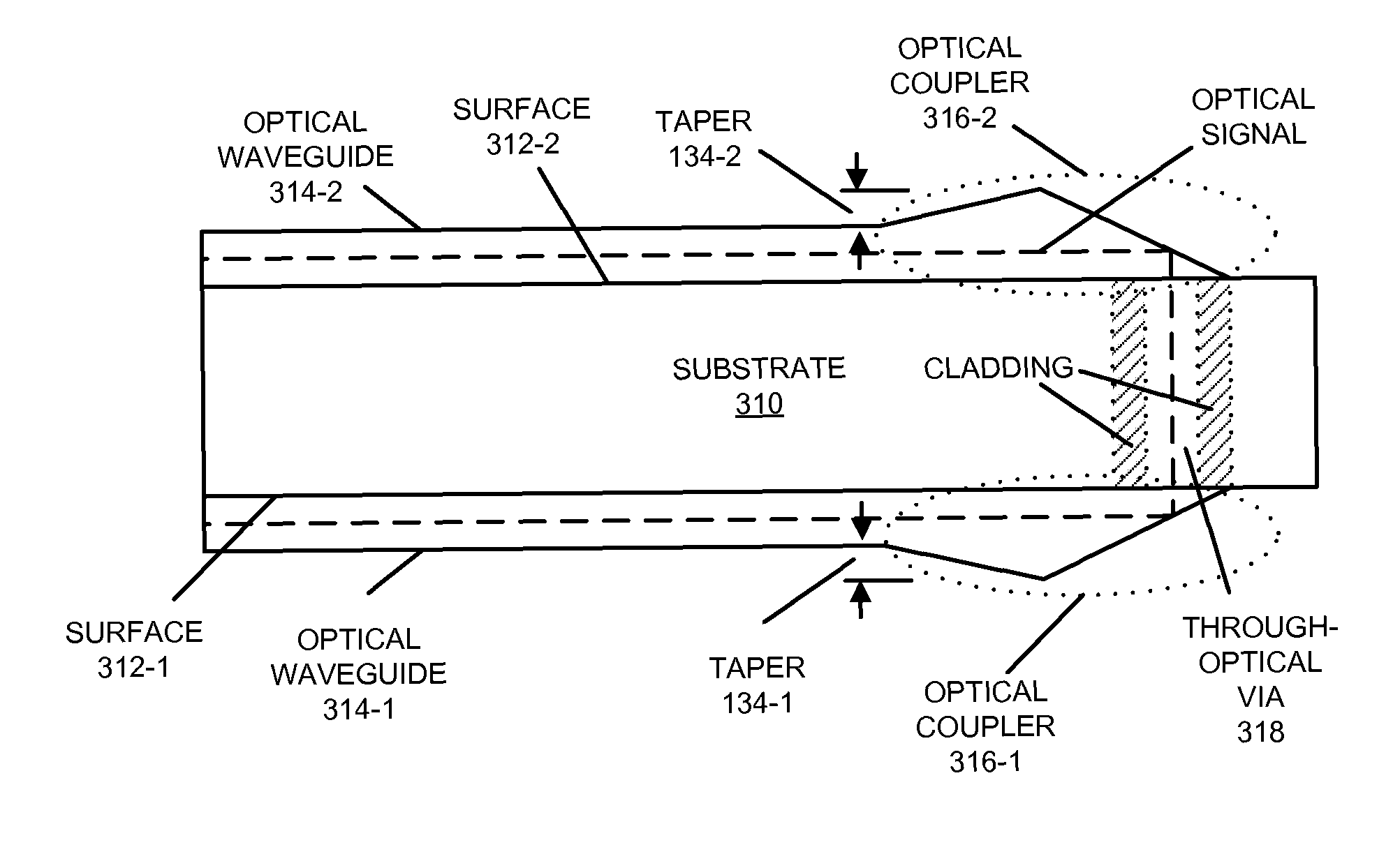
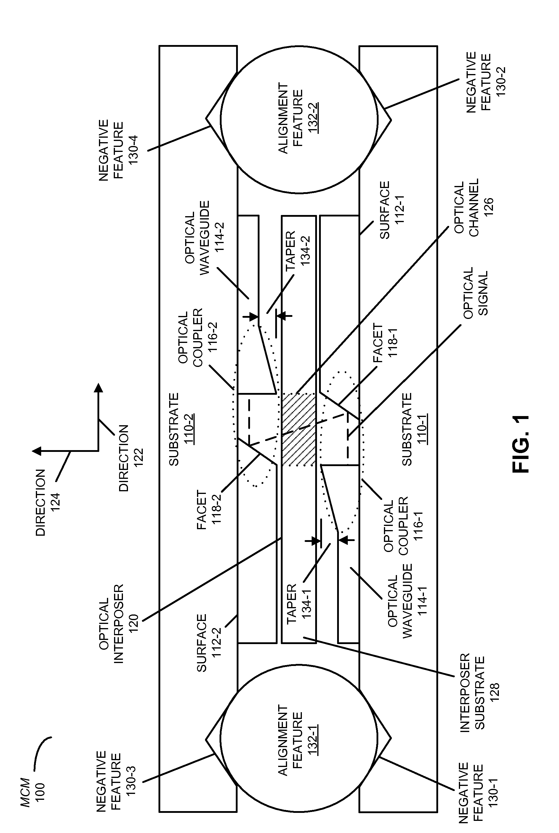
[0026]Embodiments of a multi-chip module (MCM), a system that includes the MCM, and a method for directly optically coupling an optical signal between substrates or chips in the MCM are described. In this MCM, the optical signal is conveyed by an optical waveguide disposed on a surface of a first substrate to a first optical coupler. This first optical coupler redirects the optical signal out of the plane of the optical waveguide. Then, an optical interposer guides the optical signal between the first optical coupler and a second optical coupler on a surface of a second substrate, thereby reducing spatial expansion of the optical signal between the optical couplers. Moreover, the second optical coupler redirects the optical signal into a plane of an optical waveguide disposed on a surface of the second substrate, which then conveys the optical signal.

[0027]By facilitating direct optical coupling of the optical signal, the MCM may facilitate high-fidelity signaling between the substr...


PUM


Abstract

In an MCM, an optical signal is conveyed by an optical waveguide disposed on a surface of a first substrate to a first optical coupler. This first optical coupler redirects the optical signal out of the plane of the optical waveguide. Then, an optical interposer guides the optical signal between the first optical coupler and a second optical coupler on a surface of a second substrate, thereby reducing spatial expansion of the optical signal between the optical couplers. Moreover, the second optical coupler redirects the optical signal into a plane of an optical waveguide disposed on a surface of the second substrate, which then conveys the optical signal.

Description

GOVERNMENT LICENSE RIGHTS[0001]This invention was made with Government support under Agreement No. HR0011-08-9-0001 awarded by DARPA. The Government has certain rights in the invention.BACKGROUND[0002]1. Field[0003]The present disclosure generally relates to the design of multi-chip modules (MCMs). More specifically, the present disclosure relates to an MCM that couples an optical signal between optical waveguides on different substrates using an optical interposer.[0004]2. Related Art[0005]Optical signaling based on silicon photonics has the potential to alleviate off-chip bandwidth bottlenecks, as well as to provide low latency chip-to-chip communication. Interconnects with these capabilities can facilitate new system architectures that include multiple chips, with multi-threaded cores. For maximal density, the physical package for such a system may employ a combination of planar packaging and vertical chip stacking as needed. An example of such a system is a multi-chip module (MC...

Claims


Application Information

Patent Timeline
Patent Type & Authority Patents(United States)
IPC IPC(8): G02B6/00G02B6/26G02B6/42G02B6/12
CPCG02B6/1228G02B6/12004
Inventor RAJ, KANNANCUNNINGHAM, JOHN E.THACKER, HIREN D.
Owner ORACLE INT CORP
Why Eureka
Try Eureka