Conductive paste and mold for electrical connection of photovoltaic die to substrate
- Summary
- Abstract
- Description
- Claims
- Application Information
AI Technical Summary
Benefits of technology
Problems solved by technology
Method used
Image

Examples
Embodiment Construction
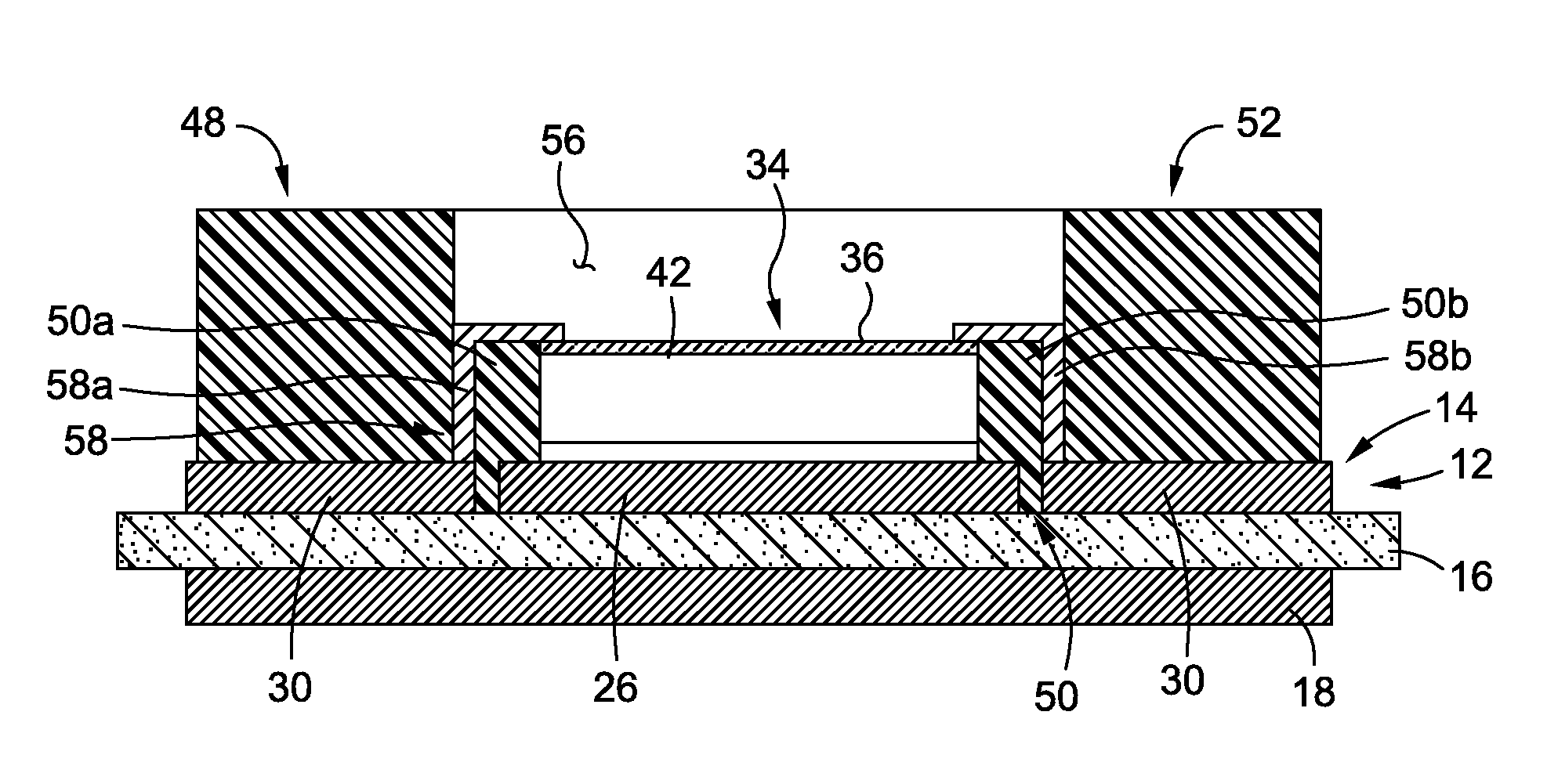
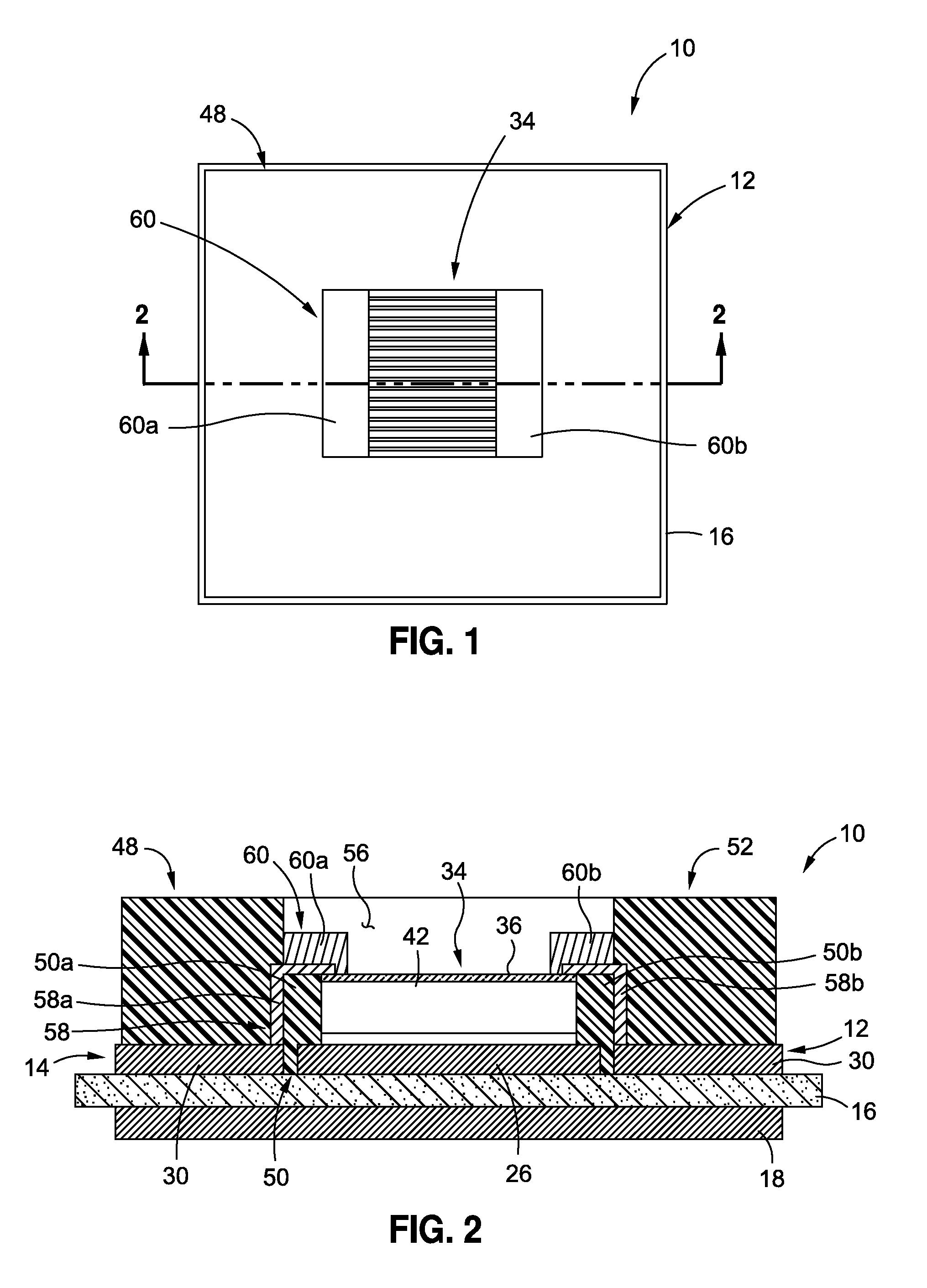
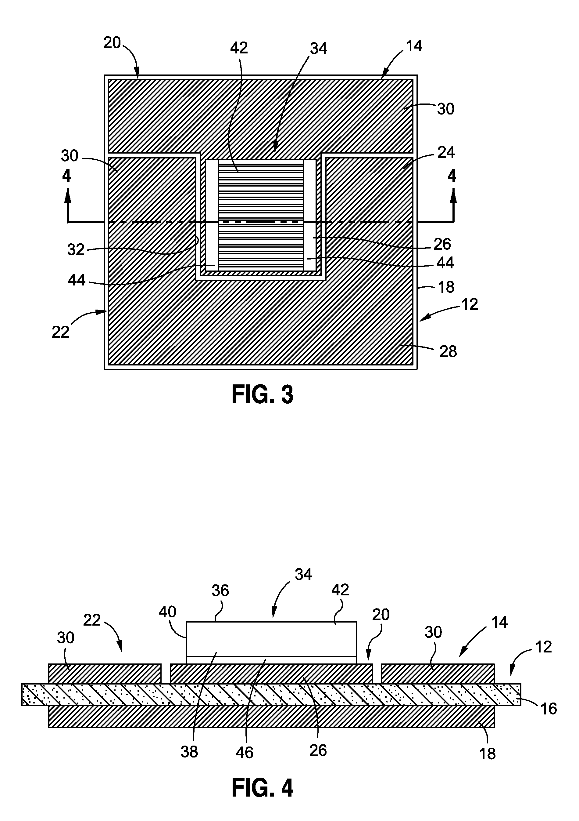
[0021]Referring now to the drawings wherein the showings are for purposes of illustrating a preferred embodiment of the present invention only, and not for purposes of limiting the same, FIGS. 1-8 depict a concentrated photovoltaic (CPV) package or module 10 constructed in accordance with the present invention. In FIGS. 1 and 2, the CPV module 10 is depicted in its fully fabricated state. In FIGS. 3-8, the CPV module 10 is depicted in partially completed states of fabrication, with an initial fabrication stage being shown in FIGS. 3 and 4, an intermediate fabrication stage being shown in FIGS. 5 and 6, and an intermediate fabrication stage just prior to completion being shown in FIGS. 7 and 8.
[0022]As is most easily seen in FIGS. 3 and 4, the CPV module 10 comprises a substrate 12 which has a generally quadrangular (e.g., square) configuration. When viewed from the perspective shown in FIG. 4, the substrate 12 comprises a first (top) layer 14 which is preferably fabricated from copp...
PUM
 Abstract
Description
Claims
Application Information
 - R&D Engineer
- R&D Manager
- IP Professional
- Industry Leading Data Capabilities
- Powerful AI technology
- Patent DNA Extraction
Browse by: Latest US Patents, China's latest patents, Technical Efficacy Thesaurus, Application Domain, Technology Topic.
© 2024 PatSnap. All rights reserved.Legal|Privacy policy|Modern Slavery Act Transparency Statement|Sitemap