Three-dimensional integrated circuit design device, three-dimensional integrated circuit design, method, and program

a three-dimensional integrated circuit and design device technology, applied in computer aided design, solid-state devices, instruments, etc., can solve the problems of large design margin, drive capability, increase in the area of the entire circuit, etc., and achieve the effect of small performance margin

Inactive Publication Date: 2013-10-22
PANASONIC CORP
View PDF5 Cites 147 Cited by
  • Summary
  • Abstract
  • Description
  • Claims
  • Application Information

AI Technical Summary

Benefits of technology

[0008]According to the art disclosed in the Patent Literature 1, switching between cells is performed depending on an actual operating temperature. This requires the same number of circuits as the conditions even if some of the circuits have the same functions with overlap. Also, it is necessary to prepare a circuit for detecting an actual operating temperature. In this way, the art disclosed in the Patent Literature 1 can decrease the margin in terms of power consumption. However, this art requires an area where the circuits having the same functions with overlap are to be mounted that is larger than a reduced area margin which results from selecting a cell appropriate for an actual operating temperature. This leads to the increase in area of the entire circuit.
[0009]Also, since a three-dimensional integrated circuit is constituted by stacked semiconductor silicon chips, a difference increases between an actual operating temperature of each chip and a worst-case temperature assumed for the entire three-dimensional integrated circuit. If logic synthesis is performed based on this worst-case temperature, a three-dimensional integrated circuit is designed with use of standard cells having an excessive drive capability. This results in design of a circuit having a large performance margin.
[0012]According to the present invention, an operating temperature is calculated with respect to a chip forming each of layers constituting a three-dimensional integrated circuit to be designed, in consideration of respective heat values of respective chips forming the layers and the stack structure of each chip such as the thickness of the chip. This makes it possible to set a worst-case temperature that is close to an actual operating temperature of the chip. Furthermore, with respect to a chip forming each layer, one library is selected appropriate for the worst-case temperature among a plurality of libraries included in a standard cell library, and logic synthesis is performed on each layer with use of the selected library. This enables design of a three-dimensional integrated circuit having a small performance margin in the logic synthesis phase.

Problems solved by technology

This leads to the increase in area of the entire circuit.
If logic synthesis is performed based on this worst-case temperature, a three-dimensional integrated circuit is designed with use of standard cells having an excessive drive capability.
This results in design of a circuit having a large performance margin.

Method used


Image

  • Three-dimensional integrated circuit design device, three-dimensional integrated circuit design, method, and program
  • Three-dimensional integrated circuit design device, three-dimensional integrated circuit design, method, and program
  • Three-dimensional integrated circuit design device, three-dimensional integrated circuit design, method, and program

Examples


embodiment 1

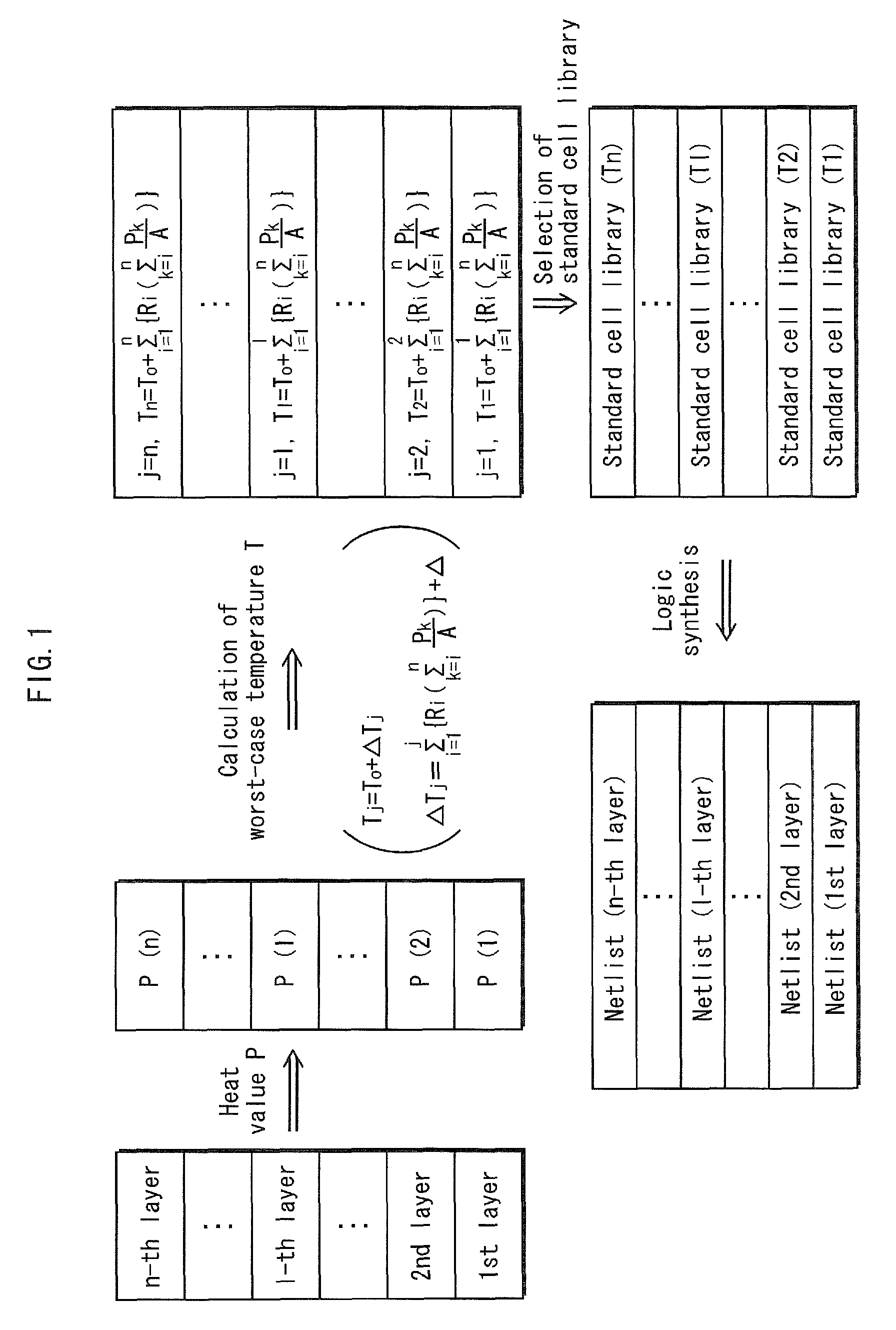
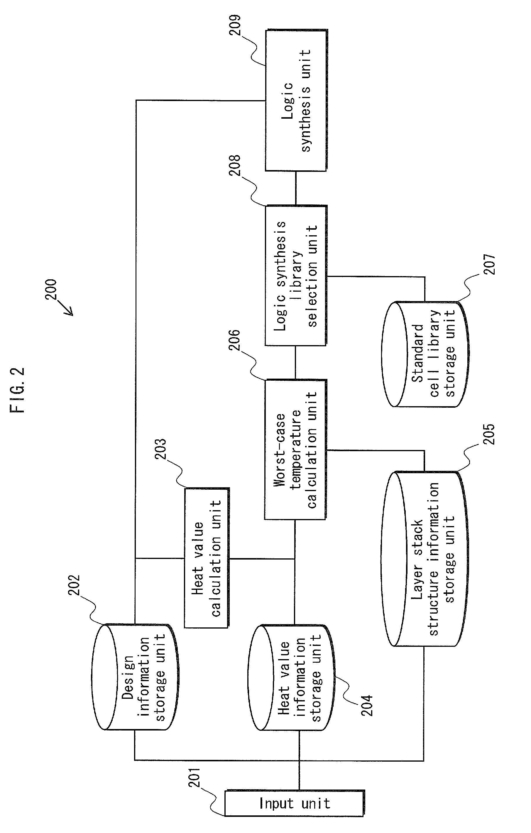
[0034]An integrated circuit design device relating to Embodiment 1 is an integrated circuit design device that designs a three-dimensional integrated circuit with use of standard cells. FIG. 1 shows the outline of processing by the integrated circuit design device relating to the Embodiment 1.

[0035]As shown in FIG. 1, firstly, based on respective heat values P of respective chips forming layers constituting a three-dimensional integrated circuit to be designed, the integrated circuit design device calculates respective worst-case temperatures T of the respective chips forming the constituting layers. The respective heat values of the respective chips forming the constituting layers, which are for use in calculating the respective worst-case temperatures T, are each calculated based on an RTL description or the like, or is externally obtained from a data sheet or the like. In equations shown in FIG. 1 for calculating the worst-case temperature T of each chip, “ΔT” represents a temper...

embodiment 2

[0077]In the same way as the integrated circuit design device 200 relating to the Embodiment 1, in the logic synthesis phase, an integrated circuit design device relating to Embodiment 2 calculates a worst-case temperature of a chip forming each of layers constituting a three-dimensional integrated circuit to be designed based on a heat value of each layer, and selects a library for each layer based on the calculated worst-case temperature to perform logic synthesis on each layer. The integrated circuit design device relating to the Embodiment 2 differs from the integrated circuit design device 200 in method of calculating the heat value of each layer. The integrated circuit design device relating to the Embodiment 2 calculates a toggle rate based on an RTL description and synthesis constraints to obtain a heat value for each layer. This enables high-speed calculation of the heat value of each layer, without RTL simulations using an operation vector. The following specifically expla...

embodiment 3

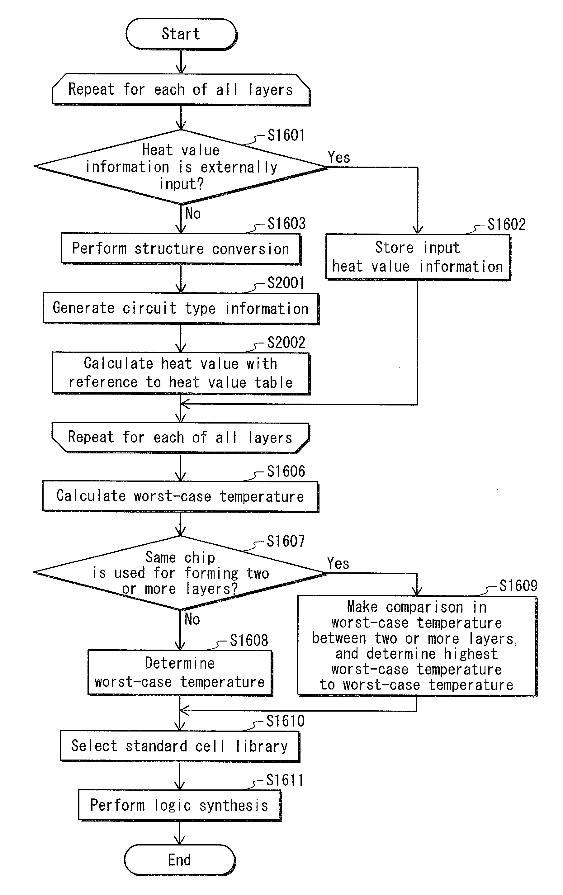
[0084]In the same way as the integrated circuit design device 200 relating to the Embodiment 1, in the logic synthesis phase, an integrated circuit design device relating to Embodiment 3 calculates a worst-case temperature of a chip forming each of layers constituting a three-dimensional integrated circuit to be designed based on a heat value of each layer, and selects a library for each layer based on the calculated worst-case temperature to perform logic synthesis on each layer. The integrated circuit design device relating to the Embodiment 3 differs from the integrated circuit design device 200 in method of calculating the heat value of each layer. The integrated circuit design device relating to the Embodiment 3 calculates the heat value of each layer, by referring to a predetermined heat value table with use of an RTL description, circuit type information indicating the circuit type of each module described in the RTL description, a circuit scale calculated for each module, an...


PUM


Abstract

A worst-case temperature calculation unit calculates, based on heat value information of each layer of a three-dimensional integrated circuit to be designed and stack structure information of the three-dimensional integrated circuit, a worst-case temperature of a layer during operation that is targeted for logic synthesis. A logic synthesis library selection unit selects a library appropriate for the calculated worst-case temperature. A logic synthesis unit performs logic synthesis on the targeted layer with use of the selected library.

Description

BACKGROUND OF INVENTION[0001]1. Technical Field[0002]The present invention relates to an art of designing a three-dimensional integrated circuit, and particularly to an art of designing a three-dimensional integrated circuit in consideration of heat generated within the three-dimensional integrated circuit.[0003]2. Background Art[0004]A three-dimensional integrated circuit has properties that heat is hard to be externally dissipated, compared to a two-dimensional integrated circuit. This makes important to design a three-dimensional integrated circuit in consideration of heat generated within the three-dimensional integrated circuit. For example, there has been known an art of making a circuit layout in the mask layout design phase such that each two vertically stacked chips do not have respective heat generating portions in the corresponding position (see Non-Patent Literature 1).[0005]Also, it is preferable, in a phase prior to the logic synthesis phase, to start such a design as ...

Claims


Application Information

Patent Timeline
Patent Type & Authority Patents(United States)
IPC IPC(8): G06F17/50
CPCH01L27/0211G06F17/505H01L27/0688G06F30/327
Inventor MORIMOTO, TAKASHIHASHIMOTO, TAKASHI
Owner PANASONIC CORP
Why Eureka
Try Eureka