Semiconductor laser device

a laser device and semiconductor technology, applied in semiconductor lasers, laser optical resonator construction, laser details, etc., can solve the problems of complex control algorithm, complicated relationship between wavelength and control current, and extensive and expensive characterization of each laser

Active Publication Date: 2013-10-29
EFFECT PHOTONICS BV
View PDF13 Cites 4 Cited by
  • Summary
  • Abstract
  • Description
  • Claims
  • Application Information

AI Technical Summary

Benefits of technology

[0009]Proposed is a tuning approach in which a laser is used that can operate only at a discrete set of equally spaced wavelengths that are matched to the internationally standardized telecommunication wavelengths (ITU-grid). The desired wavelength is selected by re-injecting a small signal at the right wavelength into the laser (filtered feedback). For this purpose a compact active discretely tunable filter (Arrayed waveguide grating (AWG)) is used. This approach yields a better stability and a simpler tuning algorithm than the schemes that are presently applied.
[0011]The laser and the feedback filter may be integrated in a small chip (<1 mm2) that can address a moderate number of wavelengths (8 or 16). This will provide a low-cost solution for large scale application in user access networks. For application in higher level networks more wavelengths are needed. The number of wavelengths of the chip may in accordance with an embodiment be extended by including a tunable Bragg reflector in the active filter, which enables to increase the total number of wavelengths with a factor of 2-4.

Problems solved by technology

The relation between wavelength and control currents is complicated, and a complex control algorithm is needed for getting stable operation at the right wavelength.
To provide the algorithm with the proper control data an extensive and expensive characterization of each laser is necessary.

Method used


Image

  • Semiconductor laser device
  • Semiconductor laser device
  • Semiconductor laser device

Examples


Embodiment Construction

Introduction

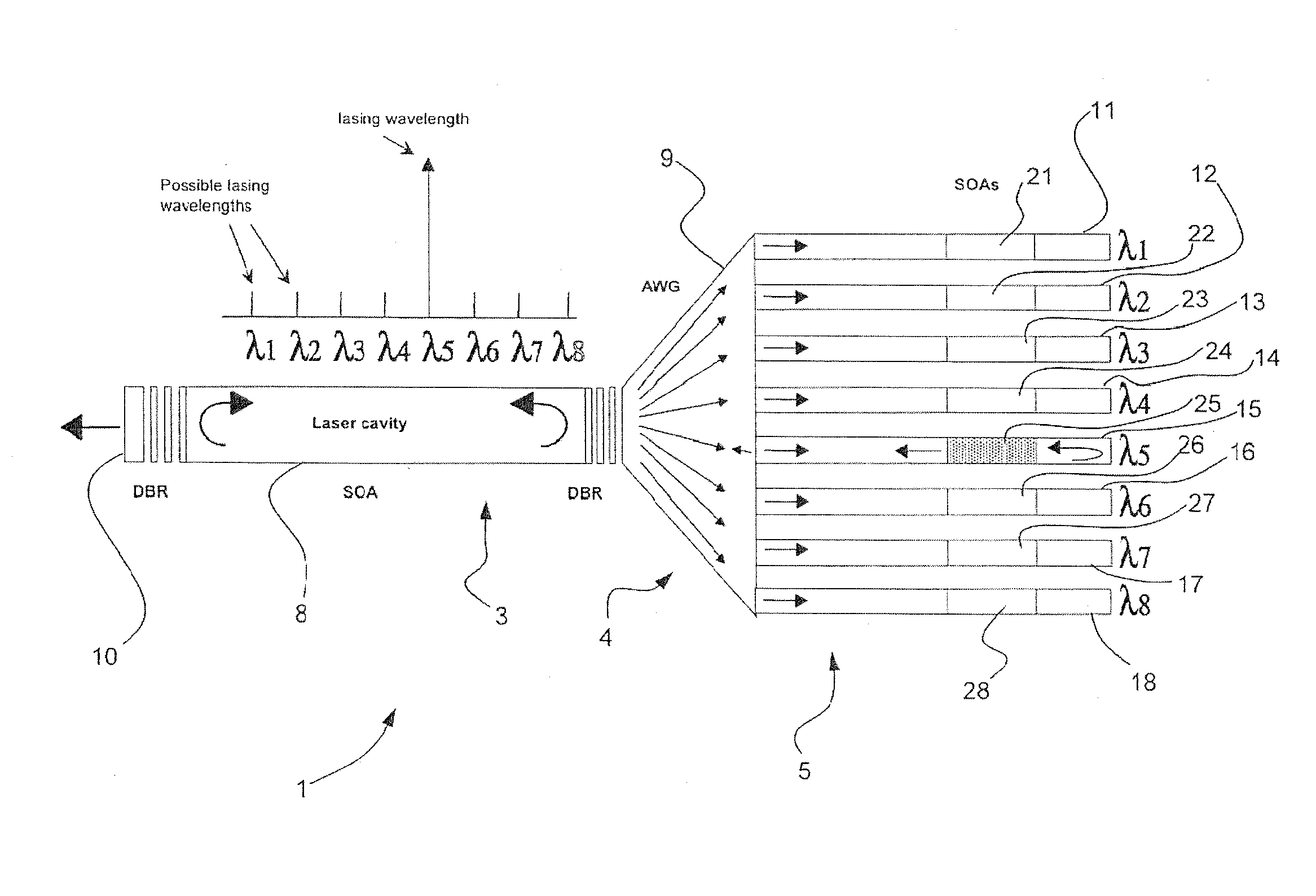
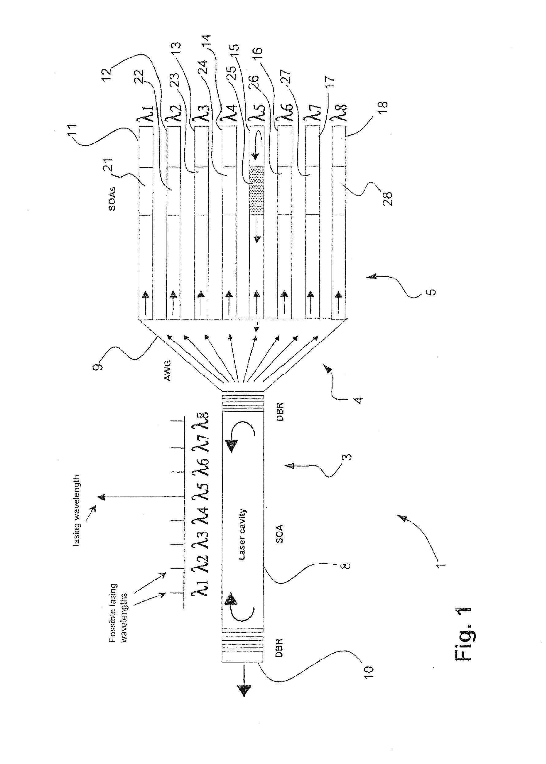
[0024]The invention provides a cheap stable integrated tunable laser, which allows the selective emission of a set of different optical wavelengths which are spaced according to the ITU grid specifications. This is an international standard for optical telecommunication frequencies. A Distributed Bragg Reflector laser (DBR-Laser) is employed in combination with an Arrayed Waveguide Grating (AWG), integrated with a set of semiconductor optical amplifiers (see FIG. 1).

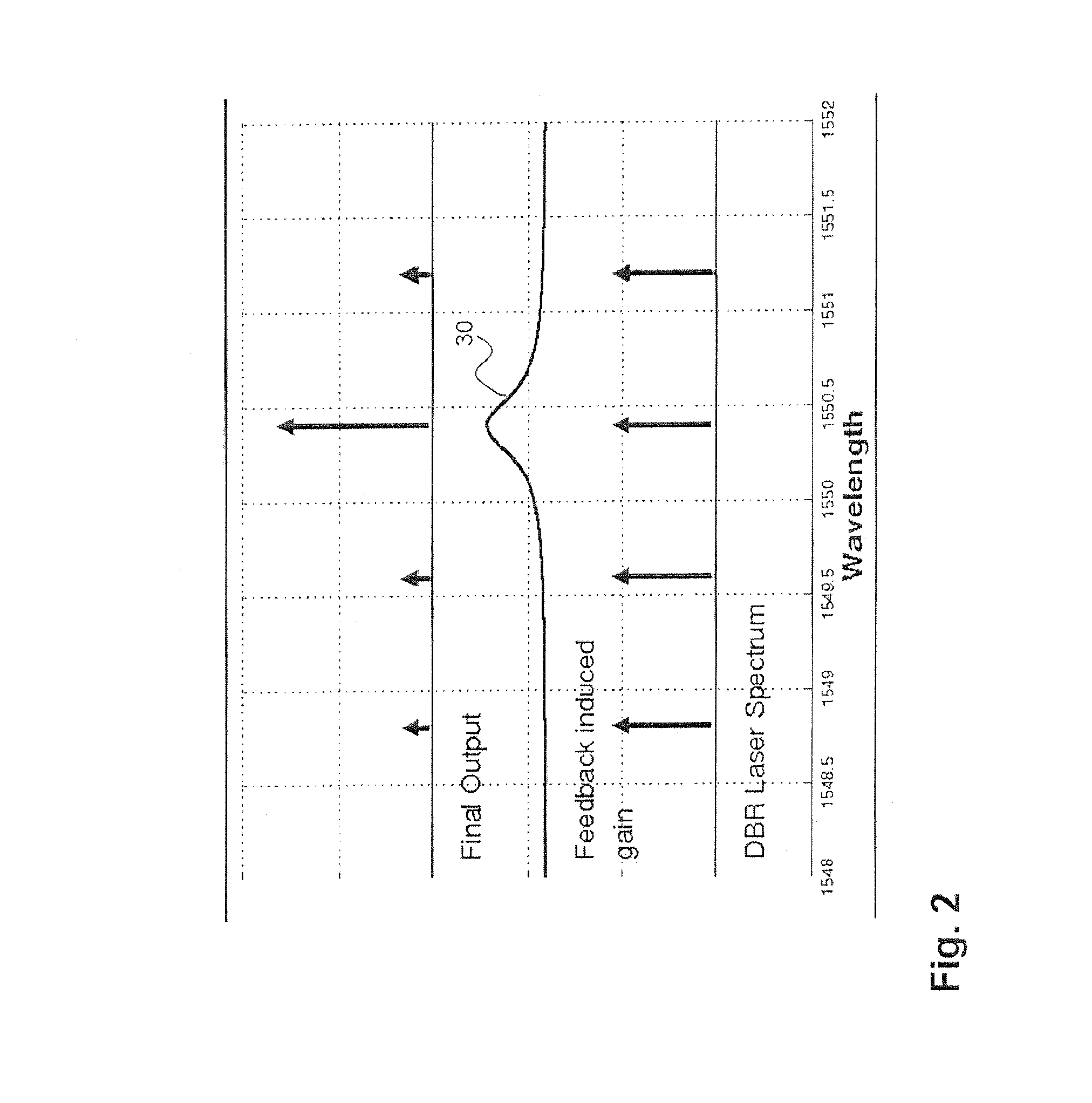
[0025]In this design, properties of the distributed Bragg reflector (DBR) mirrors are used that were previously unexploited. Distributed Bragg reflector (DBR) mirrors can be designed to provide wavelength-dependent reflectivity, with either a wide or narrow reflection bandwidth. Opposite to the standard design that focuses on achieving single mode operation through a narrow reflection bandwidth, we propose short distributed Bragg reflector (DBR) sections with wide bandwidths, which allow laser operation in se...


PUM


Abstract

The present invention is directed to a semiconductor laser device comprising a first resonator section for resonating an optical resonator signal for providing an optical output signal at an output of said laser device, wherein said first resonator section is arranged for selectively resonating at a plurality of discrete output wavelengths, and wherein said laser device further comprises a second resonator section operatively connected to said first resonator section, said second resonator section being arranged for providing an optical feedback signal at a feedback wavelength to said first resonator section for locking said first resonator section into resonating at a selected output wavelength of said discrete output wavelengths, which selected output wavelength corresponds to said feedback wavelength for providing said optical output signal.

Description

FIELD OF THE INVENTION[0001]The present invention is directed to a semiconductor laser device comprising a first resonator section for resonating an optical resonator signal for providing an optical output signal at an output of said laser device.BACKGROUND OF THE INVENTION[0002]Semiconductor laser devices as described above are generally known and widely used in many applications in a variety of industries, such as for example telecommunications industry.[0003]Today's trend in optical communications is towards extending the optical fiber network to the end user (private or business) in order to provide a broad range of services, such as telephone, television and broadband internet. Therefore, the largest growth figures in optical communication networks are expected in the access network, where large numbers of local users get direct or wireless access to the optical network. Such effort to provide local users with direct optical access is known in jargon as Fiber To The Premises (F...

Claims


Application Information

Patent Timeline
Patent Type & Authority Patents(United States)
IPC IPC(8): H01S5/0625H01S3/082H01S5/40H01S5/042H01S5/125H01S5/12
CPCH01S5/06256H01S5/065H01S5/125H01S5/0268H01S5/0656H01S5/1021H01S5/1209H01S5/4087H01S5/0425H01S5/124H01S5/1215H01S5/1212
Inventor DOCTER, BOUDEWIJNBERI, STEFANOSMIT, MEINT KOERTKAROUTA, FOUADLEIJTENS, XAVERIUS JACQUES MARIA
Owner EFFECT PHOTONICS BV
Why Eureka
Try Eureka