Light emitting device, light emitting device unit, and method for fabricating light emitting device

a light emitting device and light emitting device technology, applied in semiconductor/solid-state device manufacturing, semiconductor devices, electrical equipment, etc., can solve the problems of less reliable zener diodes, less laborious work, and failure of leds, so as to minimize the counter-electromotive force, minimize the degradation of semiconductor light emitting elements, and minimize the effect of power consumption

Inactive Publication Date: 2013-11-05
HEAVY DUTY LIGHTING LLC
View PDF20 Cites 6 Cited by
  • Summary
  • Abstract
  • Description
  • Claims
  • Application Information

AI Technical Summary

Benefits of technology

[0049]According to one aspect of the present invention, a light emitting device includes at least one light emitting device unit. The at least one light emitting device unit includes a substrate, at least one semiconductor light emitting element, and a resistor. The at least one semiconductor light emitting element is disposed on the substrate. The resistor is coupled to the at least one semiconductor light emitting element. The resistor is coupled in parallel to the at least one semiconductor light emitting element. The resistor has a resistance set at such a value that when a light emitting operation voltage for causing light emission of the at least one semiconductor light emitting element is applied to the at least one semiconductor light emitting element, a current flowing through the resistor is equal to or less than one-fiftieth of a current flowing through the at least one semiconductor light emitting element. This minimizes a counter-electromotive force that ambient light causes to the semiconductor light emitting element when the semiconductor light emitting element is in light-off state, thereby minimizing degradation of the semiconductor light emitting element. This also minimizes an increase in power consumption associated with the current that the light emitting operation voltage causes to flow through the resistor when the semiconductor light emitting element is in light-on state. This results in advantageous effects such as an elongated service life to improve reliability and minimized energy loss.
[0050]According to another aspect of the present invention, a light emitting device unit includes a substrate, at least one semiconductor light emitting element, and a resistor. The at least one semiconductor light emitting element is disposed on the substrate. The resistor is coupled to the at least one semiconductor light emitting element. The resistor is coupled in parallel to the at least one semiconductor light emitting element. The resistor has a resistance set at such a value that when a light emitting operation voltage for causing light emission of the at least one semiconductor light emitting element is applied to the at least one semiconductor light emitting element, a current flowing through the resistor is equal to or less than one-fiftieth of a current flowing through the at least one semiconductor light emitting element. This minimizes a counter-electromotive force that ambient light causes to the semiconductor light emitting element when the semiconductor light emitting element is in light-off state, thereby minimizing degradation of the semiconductor light emitting element. This also minimizes an increase in power consumption associated with the current that the light emitting operation voltage causes to flow through the resistor when the semiconductor light emitting element is in light-on state. This results in advantageous effects such as an elongated service life to improve reliability and minimized energy loss.
[0051]According to still another aspect of the present invention, a method is for fabricating a light emitting device. The light emitting device includes at least one light emitting device unit. The at least one light emitting device unit includes a substrate, at least one semiconductor light emitting element, and a resistor. The at least one semiconductor light emitting element is disposed on the substrate. The resistor is coupled to the at least one semiconductor light emitting element. The method includes forming, by printing onto the substrate, a pair of wiring electrodes to which the at least one semiconductor light emitting element and the resistor are to be coupled. The resistor is formed onto the substrate by printing so that the pair of wiring electrodes are coupled to each other. The at least one semiconductor light emitting element is arranged between the pair of wiring electrodes. An electrode of the at least one semiconductor light emitting element is coupled to the pair of wiring electrodes so as to form the at least one light emitting device unit. The wiring electrodes and the resistor are formed utilizing a printing technique. This ensures fabrication of a large light emitting device with high productivity.

Problems solved by technology

LEDs, especially gallium nitride LEDs, are subject to failure due to electrostatic discharge, that is, has a property of low reverse breakdown voltage.
Compared with resistors, however, zener diodes cannot be fabricated easily and involve more laborious work in, for example, mounting onto the LEDs.
Moreover, zener diodes are less reliable than resistors in the long run.
Thus, the resistances of the resistors to be used need to be low.
This poses a problem of large energy loss in the current flowing through the bypass resistors.
That is, a problem of large energy loss arises.

Method used


Image

  • Light emitting device, light emitting device unit, and method for fabricating light emitting device
  • Light emitting device, light emitting device unit, and method for fabricating light emitting device
  • Light emitting device, light emitting device unit, and method for fabricating light emitting device

Examples


embodiment 1

[0080]A light emitting device and light emitting device units according to this embodiment will be described by referring to FIG. 1 through FIG. 3.

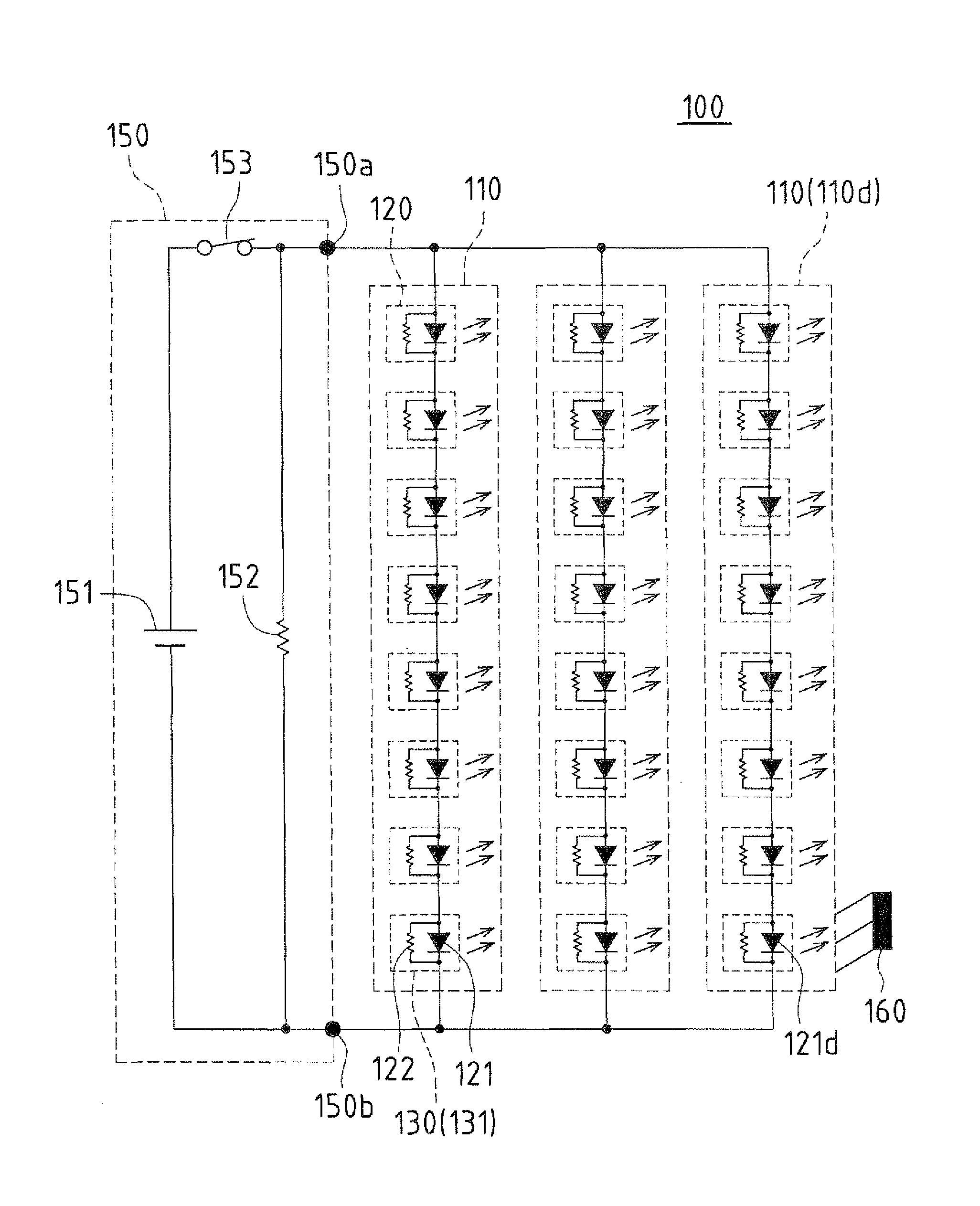
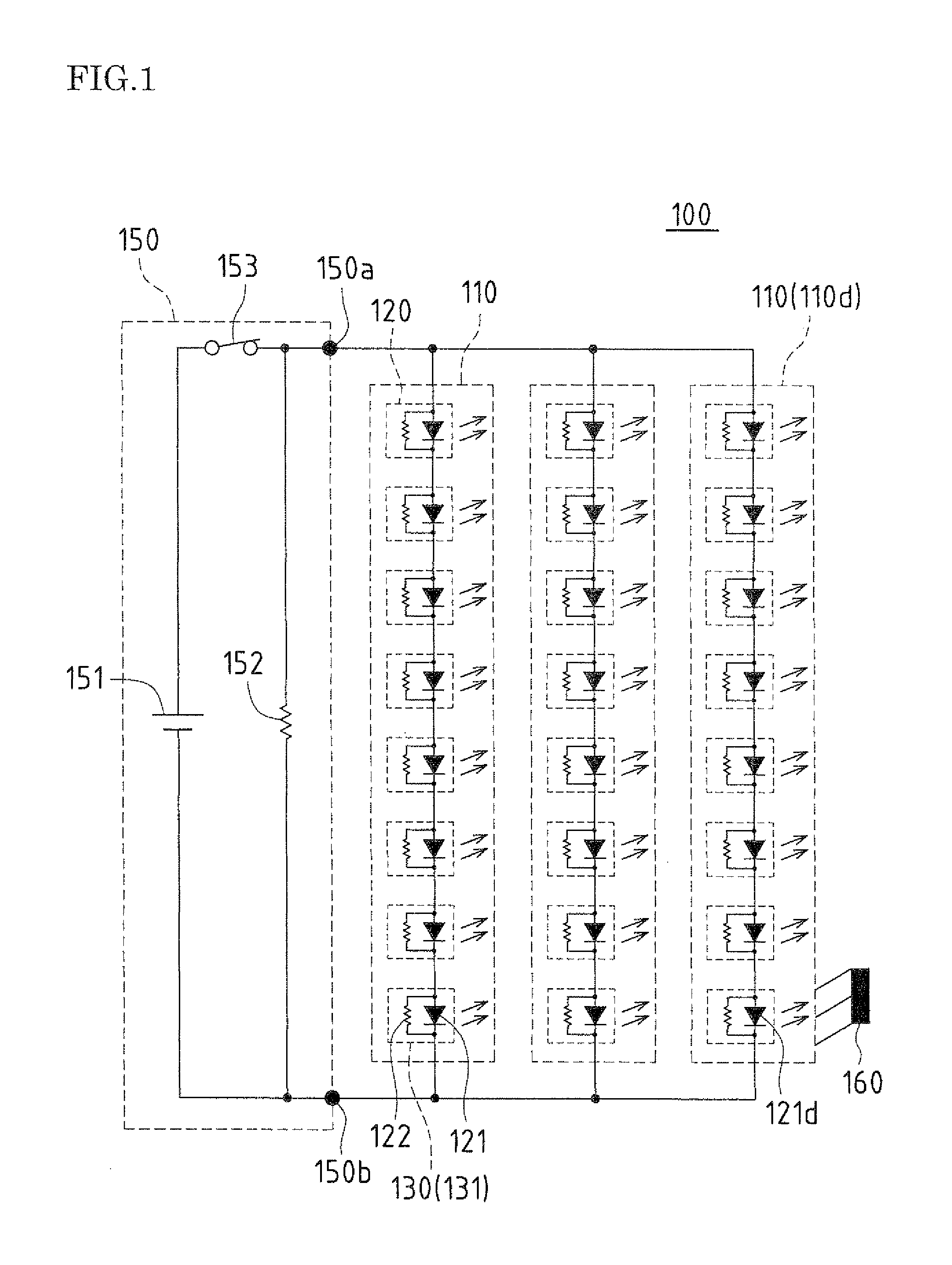
[0081]FIG. 1 is a circuit diagram of a light emitting device and light emitting device units according to embodiment 1 of the present invention.

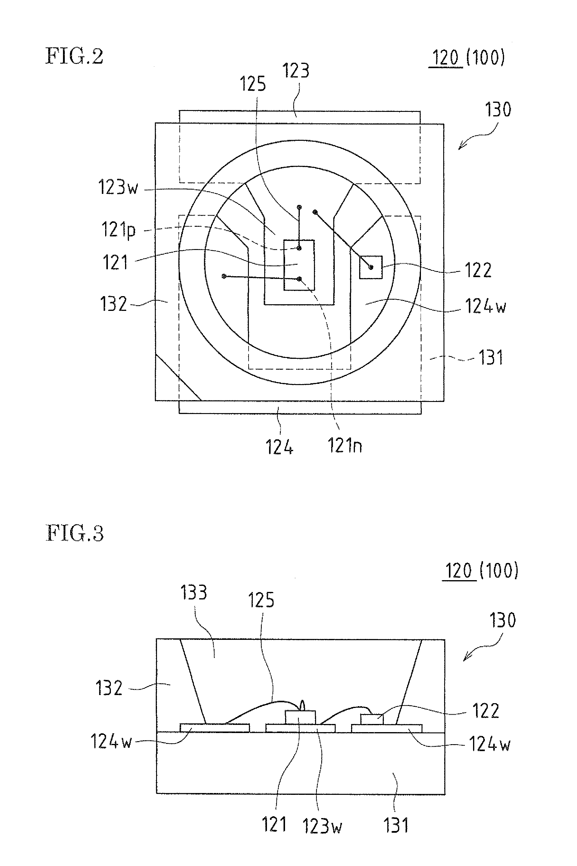
[0082]FIG. 2 is a plan view of a light emitting device unit, as seen on its light emitting surface side, which constitutes the light emitting device shown in FIG. 1.

[0083]FIG. 3 is a see-through side view of the light emitting device unit shown in FIG. 2, with a center portion of the light emitting device unit made seen through.

[0084]A light emitting device 100 according to this embodiment includes light emitting device units 120 each including a substrate 131, semiconductor light emitting elements 121 disposed on the substrate 131, and resistors 122 coupled to the respective semiconductor light emitting elements 121.

[0085]In the light emitting device 100 according to this embodiment, each resisto...

embodiment 2

[0130]A light emitting device and a light emitting device unit according to this embodiment will be described by referring to FIG. 4 and FIG. 5. The basic configuration is similar to that in embodiment 1 and thus will not be elaborated here.

[0131]FIG. 4 is a circuit diagram of a light emitting device and light emitting device units according to embodiment 2 of the present invention.

[0132]FIG. 5 is a diagram illustrating a light emitting device unit and a second composite light emitting device unit that constitute the light emitting device shown in FIG. 4, with (A) showing a plan view to illustrate a plan condition as seen on the light emitting surface side, and (B) showing an enlarged see-through side view to illustrate an enlarged side surface condition as seen through from arrow B of (A).

[0133]A light emitting device 200 according to this embodiment includes light emitting device units 220 each including a substrate 231, light emitting elements 221 on the substrate 231, and a resi...

embodiment 3

[0165]Referring to FIG. 6A through FIG. 6G, a third embodiment (method for fabricating the light emitting device, method for fabricating the second composite light emitting device unit) will be described as a method (fabrication process) for fabricating the light emitting device 200 (second composite light emitting device unit 210) according to embodiment 2. The light emitting device 200 in FIG. 6B through FIG. 6G is shown for the purpose of describing the steps and thus in a simplified form.

[0166]FIG. 6A is a flowchart schematically showing a method for fabricating a light emitting device, according to embodiment 3 of the present invention.

[0167]The method for fabricating the light emitting device 200 includes step S1 (separation groove forming step) through step S9 (dam sheet removing step).

[0168]Specifically, step S1 is a separation groove forming step shown in FIG. 6B. Step S2 is a wiring electrode forming step (wire printing, drying, and sintering step) shown in FIG. 6C. Step S...


PUM


Abstract

In a light emitting device, a light emitting device unit, and a method for fabricating a light emitting device according to an embodiment of the present invention, a light emitting device (100) includes a substrate (131), a semiconductor light emitting element (121) disposed on the substrate (131), and a resistor (122) coupled to the semiconductor light emitting element (121). The resistor (122) is coupled in parallel to the semiconductor light emitting element (121). The resistor (122) has a resistance set at such a value that when a light emitting operation voltage for causing light emission of the semiconductor light emitting element (121) is applied to the semiconductor light emitting element (121), a current flowing through the resistor (122) is equal to or less than one-fiftieth of a current flowing through the semiconductor light emitting element (121).

Description

[0001]This application is the U.S. national phase of International Application No. PCT / JP2010 / 053046 filed 26 Feb. 2010 which designated the U.S. and claims priority to JP Patent Application No. 2009-049634 filed 3 Mar. 2009, the entire contents of each of which are hereby incorporated by reference.TECHNICAL FIELD[0002]The present invention relates to a light emitting device that includes a light emitting device unit including a semiconductor light emitting element (LED) disposed on a substrate and a resistor coupled to the LED, relates to a light emitting device unit constituting the light emitting device, and relates to a method for fabricating the light emitting device.BACKGROUND ART[0003]LEDs (Light Emitting Diodes), with their recent improvements in efficiency, have come into widespread use in backlights of display devices and in lighting equipment, as energy saving light sources over light bulbs and fluorescent lights. In such applications, energy efficiency is very important....

Claims


Application Information

Patent Timeline
Patent Type & Authority Patents(United States)
IPC IPC(8): H01L33/08
CPCH01L25/167H01L25/0753H01L2924/3011H01L2224/48091H01L2924/00014H01L2924/3025H01L2924/00
Inventor ITO, MASAYUKIMIYATA, MASATAKAYAMAMURO, TAROYOKOTA, SYOJI
Owner HEAVY DUTY LIGHTING LLC
Why Eureka
Try Eureka