Si photodiode with symmetry layout and deep well bias in CMOS technology

a silicon photodiode and symmetry layout technology, applied in the field of photodiodes, can solve the problems of low responsivity of surface pd, significant affecting response performance, and limited bandwidth, and achieve the effect of increasing frequency bandwidth, reducing fabrication costs, and effective response speed of silicon photodiodes

Inactive Publication Date: 2013-12-03
NAT CENT UNIV
View PDF5 Cites 27 Cited by
  • Summary
  • Abstract
  • Description
  • Claims
  • Application Information

AI Technical Summary

Benefits of technology

[0007]The invention is directed to a silicon photodiode fabricated in CMOS technology, where the novel structure eliminates the slow diffusion carriers, increases the frequency bandwidth, and includes deep well bias and symmetry layout, such that the response speed of the silicon photodiode is increased effectively and the fabrication cost is greatly reduced.

Problems solved by technology

However, light penetration depth of Si at 850-nm is larger than 10 μm that results in low responsivity for a surface PD.
Moreover, carriers generated from bulk silicon substrate slowly diffuse to be collected and significantly affect the response performance.
The resulting bandwidth is limited.
However, the response time is still limited by the slow diffusion carriers in the substrate.
As a result, silicon photodiodes fabricated on silicon-on-insulator (SOI) substrates present the best performance, but the cost and popularity of SOI wafers are two issues.

Method used


Image

  • Si photodiode with symmetry layout and deep well bias in CMOS technology
  • Si photodiode with symmetry layout and deep well bias in CMOS technology
  • Si photodiode with symmetry layout and deep well bias in CMOS technology

Examples


Embodiment Construction

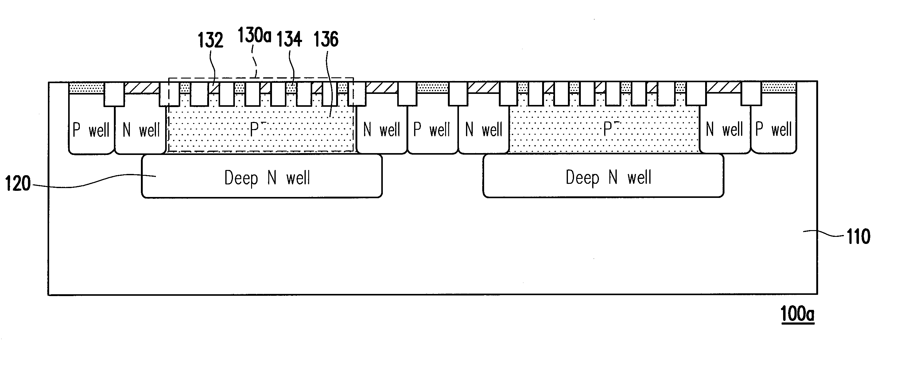
[0028]Silicon photodiodes are one of the most important devices in optical communication and are responsible for converting optical signals into electrical signals. However, when the material of a lower substrate of a silicon photodiode absorbs the absorption wavelengths of the silicon photodiode, the slow diffusion carriers from the substrate then becomes a problem which leads to slow response speed.

[0029]In an exemplary embodiment of the invention, the silicon photodiode adopts a deep well fabrication step and eliminates the effects and interferences generated after the substrate absorbs light by providing an extra deep well bias, such that the response speed and the frequency bandwidth are greatly improved. Moreover, in an exemplary embodiment of the invention, the silicon photodiode has a symmetrical surrounding structure for obtaining uniform electric field distribution. The interference from the noise of the substrate of the silicon photodiode is also reduced effectively.

[0030...


PUM


Abstract

A silicon photodiode with symmetry layout and deep well bias in CMOS technology is provided. The silicon photodiode includes a substrate, a deep well, and a PN diode structure. The deep well is disposed on the substrate, where an extra bias is applied to the deep well. The region surrounded by the deep well forms the main body of the silicon photodiode. The PN diode structure is located in the region surrounded by the deep well, where the silicon photodiode has a symmetry layout. The deep well is adopted when fabricating the silicon photodiode, and the extra bias is applied to the deep well to eliminate the interference and effect of the substrate absorbing light, and further greatly improve speed and bandwidth. Furthermore, the silicon photodiode has a symmetry layout, so that uniform electric field distribution is achieved, and the interference of the substrate noise is also reduced.

Description

CROSS-REFERENCE TO RELATED APPLICATION[0001]This application claims the priority benefit of Taiwan application serial no. 100100499, filed Jan. 6, 2011. The entirety of the above-mentioned patent application is hereby incorporated by reference herein and made a part of this specification.BACKGROUND OF THE INVENTION[0002]1. Field of the Invention[0003]The invention relates to a photodiode and more particularly to a silicon photodiode with symmetry layout and deep well bias in CMOS technology.[0004]2. Description of Related Art[0005]Nowadays, Si photodiodes (PDs) fabricated by complementary metal-oxide-semiconductor (CMOS) become popular in the application of optical communication at near-infrared wavelengths (e.g. 850-nm) due to its low cost and possible integration with receivers. However, light penetration depth of Si at 850-nm is larger than 10 μm that results in low responsivity for a surface PD. Moreover, carriers generated from bulk silicon substrate slowly diffuse to be collec...

Claims


Application Information

Patent Timeline
Patent Type & Authority Patents(United States)
IPC IPC(8): H01L31/113
CPCH01L31/103H01L27/1446
Inventor HSIN, YUE-MINGCHOU, FANG-PINGWANG, CHING-WENCHEN, GUAN-YU
Owner NAT CENT UNIV
Why Eureka
Try Eureka