Eureka AIR delivers breakthrough ideas for toughest innovation challenges, trusted by R&D personnel around the world.

Asymmetric mesh NoC topologies

a topology and mesh technology, applied in the field of interconnect architecture, can solve the problems of complex analysis of routing form, low efficiency of routing, and low efficiency of routing, and achieve the effects of avoiding the use of adaptive routing in practice, and increasing the number of components on the chip

Inactive Publication Date: 2013-12-03
INTEL CORP
View PDF18 Cites 115 Cited by
  • Summary
  • Abstract
  • Description
  • Claims
  • Application Information

AI Technical Summary

Benefits of technology

The patent text describes a technique for creating customized topologies for chip interconnects that are aware of the physical design and can route signals efficiently. This technique helps to avoid deadlocks and minimize delays in the signal transmission process. Overall, the patent provides a solution for creating efficient and effective interconnects for chips.

Problems solved by technology

The number of components on a chip is rapidly growing due to increasing levels of integration, system complexity and shrinking transistor geometry.
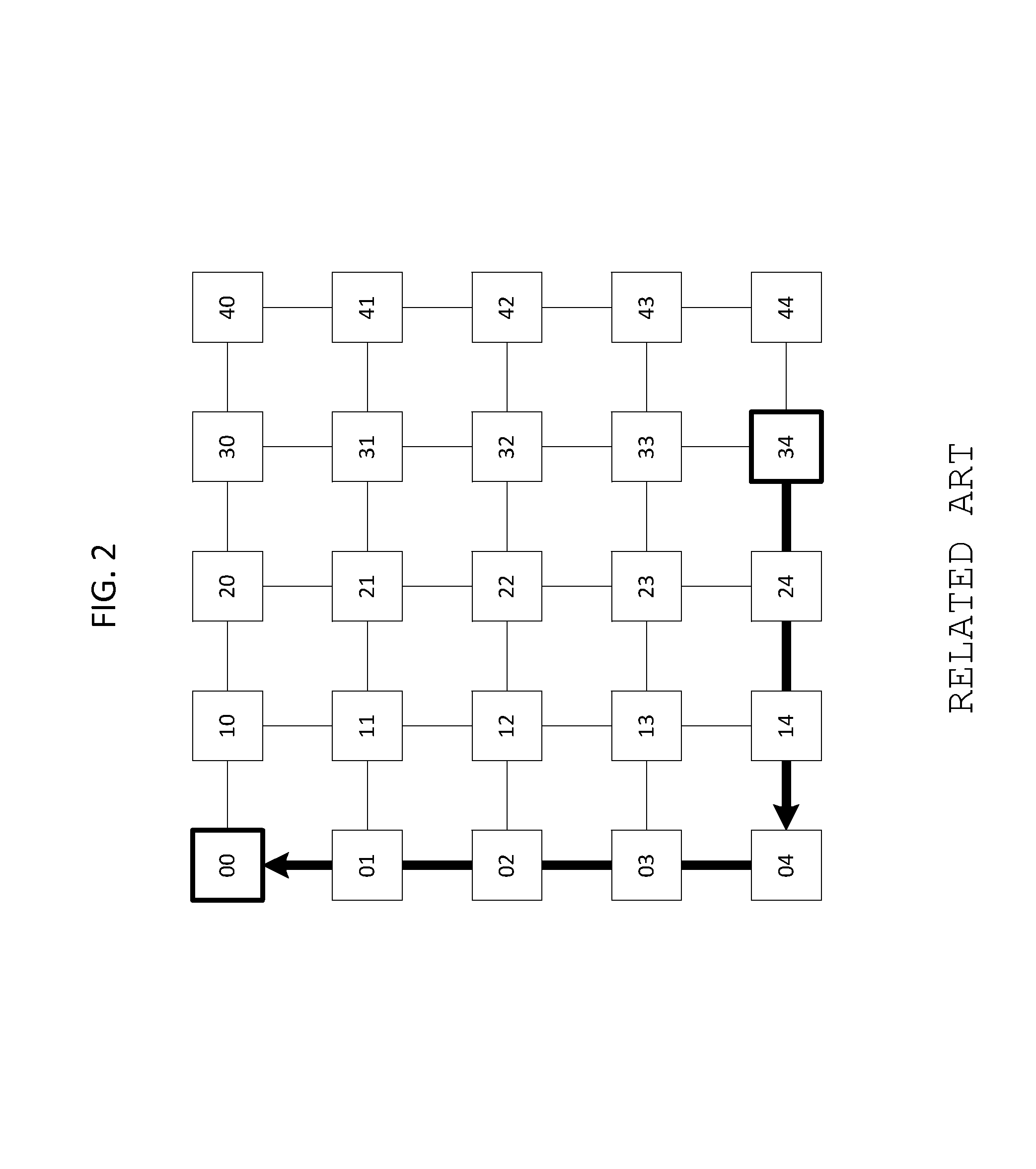
This form of routing may be complex to analyze for deadlocks and have complexities associated with maintaining packet ordering.
Because of these implementation challenges, adaptive routing is rarely used in practice.
Further, the blocks may have restrictions on allowing interconnect infrastructure amidst its internal logic and wires.
These restrictions mean that interconnect wires on practical chips cannot be as regular and structured as a 2D-mesh topology.
This approach can create significant problems during the chip's physical design phase.
The system interconnect can place large demands on metal / wiring resources and routing channels on the die.
Further, ad hoc layout of the interconnect can cause wiring congestions on the die and can aggravate cross-talk and SI related issues.
Routing around blockages can result in unpredictable inter-router wire lengths causing timing paths within the interconnect to show large negative slacks in top level timing.

Method used


Image

  • Asymmetric mesh NoC topologies
  • Asymmetric mesh NoC topologies
  • Asymmetric mesh NoC topologies

Examples


Embodiment Construction

[0031]FIG. 3 illustrates an example of uniform (e.g., homogeneous) cores 301 connected by a full regular mesh topology consisting of routers 302 and physical links 303. Contrast this to FIG. 4 which illustrates blocks of heterogeneous size and shapes interconnected using a customized mesh topology. The customized mesh is adapted from a full mesh by selectively removing one or more routers and / or one or more links from a full mesh, to produce a resultant sparsely populated mesh. This derivative mesh topology with an irregular structure will be referred to herein as a “sparse mesh”.

[0032]An option for interconnecting heterogeneous blocks is to use a network of routers in an ad hoc topology. Such a topology would need each router to be fully identified by a network ID and routing algorithm over the network would have to be fully flexible, requiring complex source routing or distributed table based routing. Compared to this approach, the present inventive concept uses a regular mesh as ...


PUM


Abstract

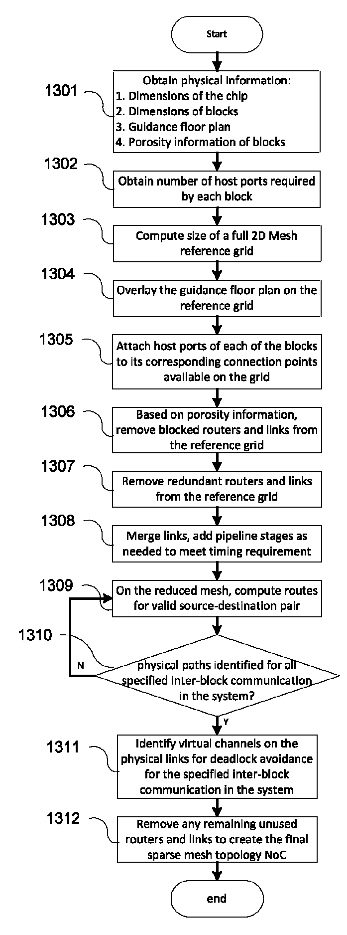
A method of interconnecting blocks of heterogeneous dimensions using a NoC interconnect with sparse mesh topology includes determining a size of a mesh reference grid based on dimensions of the chip, dimensions of the blocks of heterogeneous dimensions, relative placement of the blocks and a number of host ports required for each of the blocks of heterogeneous dimensions, overlaying the blocks of heterogeneous dimensions on the mesh reference grid based on based on a guidance floor plan for placement of the blocks of heterogeneous dimensions, removing ones of a plurality of nodes and corresponding ones of links to the ones of the plurality of nodes which are blocked by the overlaid blocks of heterogeneous dimensions, based on porosity information of the blocks of heterogeneous dimensions, and mapping inter-block communication of the network-on-chip architecture over remaining ones of the nodes and corresponding remaining ones of the links.

Description

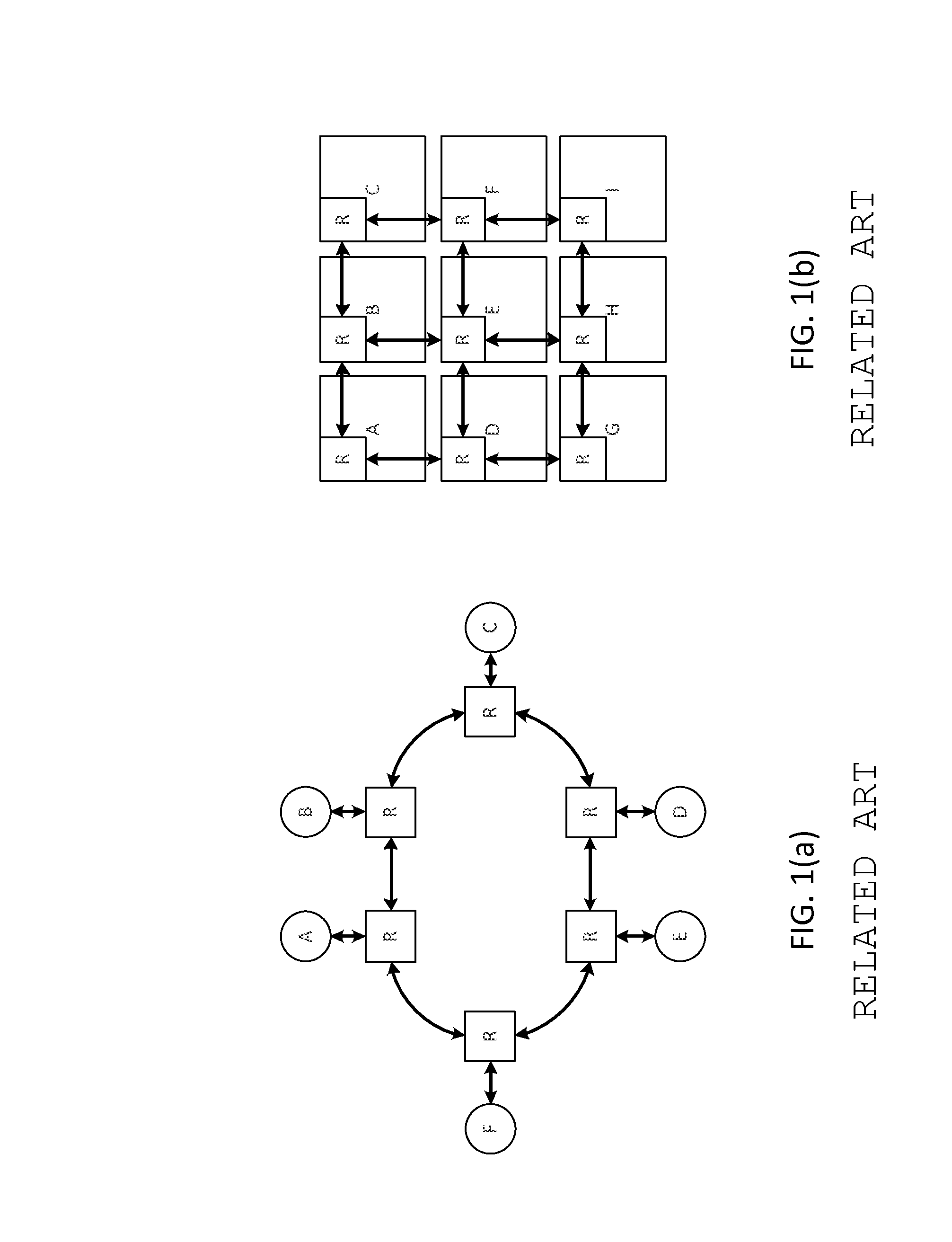
BACKGROUND[0001]1. Technical Field[0002]Methods and example embodiments described herein are generally directed to interconnect architecture, and more specifically, to network-on-chip system interconnect architecture.[0003]2. Related Art[0004]The number of components on a chip is rapidly growing due to increasing levels of integration, system complexity and shrinking transistor geometry. Complex System-on-Chips (SoCs) may involve a variety of components e.g., processor cores, DSPs, hardware accelerators, memory and I / O, while Chip Multi-Processors (CMPs) may involve a large number of homogenous processor cores, memory and I / O subsystems. In both systems, the on-chip interconnect plays a key role in providing high-performance communication between the various components.[0005]Due to scalability limitations of traditional buses and crossbar based interconnects, Network-on-Chip (NoC) has emerged as a paradigm to interconnect a large number of components on the chip. NoC is a global sha...

Claims


Application Information

Patent Timeline
IPC IPC(8): G06F17/50
CPCG06F17/5072G06F17/5077G06F15/7825G06F15/76G06F13/40G06F17/5054G06F17/5027G06F2217/40G06F2217/66H04L12/28H03K17/00G06Q10/047G06K9/00979H04L12/66H04Q3/52G06F2115/08G06F30/392G06F30/394G06F30/34G06F30/331G06F2113/18G06V10/95
Inventor PHILIP, JOJIKUMAR, SAILESHNORIGE, ERICHASSAN, MAHMUDMITRA, SUNDARI
Owner INTEL CORP
Why Eureka
Eureka Blog
Learn More