Plasma confinement apparatus, and method for confining a plasma

a technology of confinement apparatus and plasma, which is applied in the direction of plasma technique, coating, electric discharge lamp, etc., can solve the problems of shortening the lifespan of the reaction chamber or its components, contaminating the surface of any semiconductor substrate being processed in the chamber, and lowering the performance and yield rate that can be produced from the same reaction chamber

Active Publication Date: 2013-12-17
ADVANCED MICRO FAB EQUIP INC CHINA
View PDF16 Cites 7 Cited by
  • Summary
  • Abstract
  • Description
  • Claims
  • Application Information

AI Technical Summary

Problems solved by technology

If this occurs, erosion or deposition may take place in these remote regions causing a resulting particle contamination in the reaction chamber thus lowering the performance and yield rates that can be produced from the same reaction chamber.
Still further, this deposition and erosion may shorten the lifespan of the reaction chamber or its components.
In addition to the foregoing, if plasma is not confined within the processing region charged particles produced by the plasma may collide with unprotected regions of the reaction chamber causing further impurities, particulate matter, and contamination to be generated and which may result in the contamination of the surface of any semiconductor substrates which are being processed in the chamber.
While this arrangement has operated with some degree of success, its principal shortcoming is that if the magnetic field of the magnet is too strong, it may potentially damage electrically sensitive components which are located on a semiconductor substrate that is being processed.
Obviously, if the magnet employed with such an assembly is too weak, the plasma diffusion cannot be effectively confined, and the resulting contamination, noted above, results.
However, the principal shortcoming in this device is that this arrangement cannot completely prevent charged particles from leaking outside the processing region nor can it completely prevent the leakage of electromagnetic waves or prevent a secondary radio frequency discharge of the leaked charged particles outside the processing region.
Consequently, contamination can still be generated.
This unwanted plasma is caused by the electric field outside the processing region.
In practice, however, this method has shown that it cannot completely prevent the formation of an electric field outside the processing region.
While this device works with some degree of success it should be understood that the collision of ions of the plasma onto the surface of the conductive sealing ring may cause contamination to be generated in the chamber, and other electrical discharges.

Method used


Image

  • Plasma confinement apparatus, and method for confining a plasma
  • Plasma confinement apparatus, and method for confining a plasma
  • Plasma confinement apparatus, and method for confining a plasma

Examples


Embodiment Construction

[0028]This disclosure of the invention is submitted in furtherance of the constitutional purposes of the U.S. Patent Laws “to promote the progress of science and useful arts” (Article 1, Section 8).

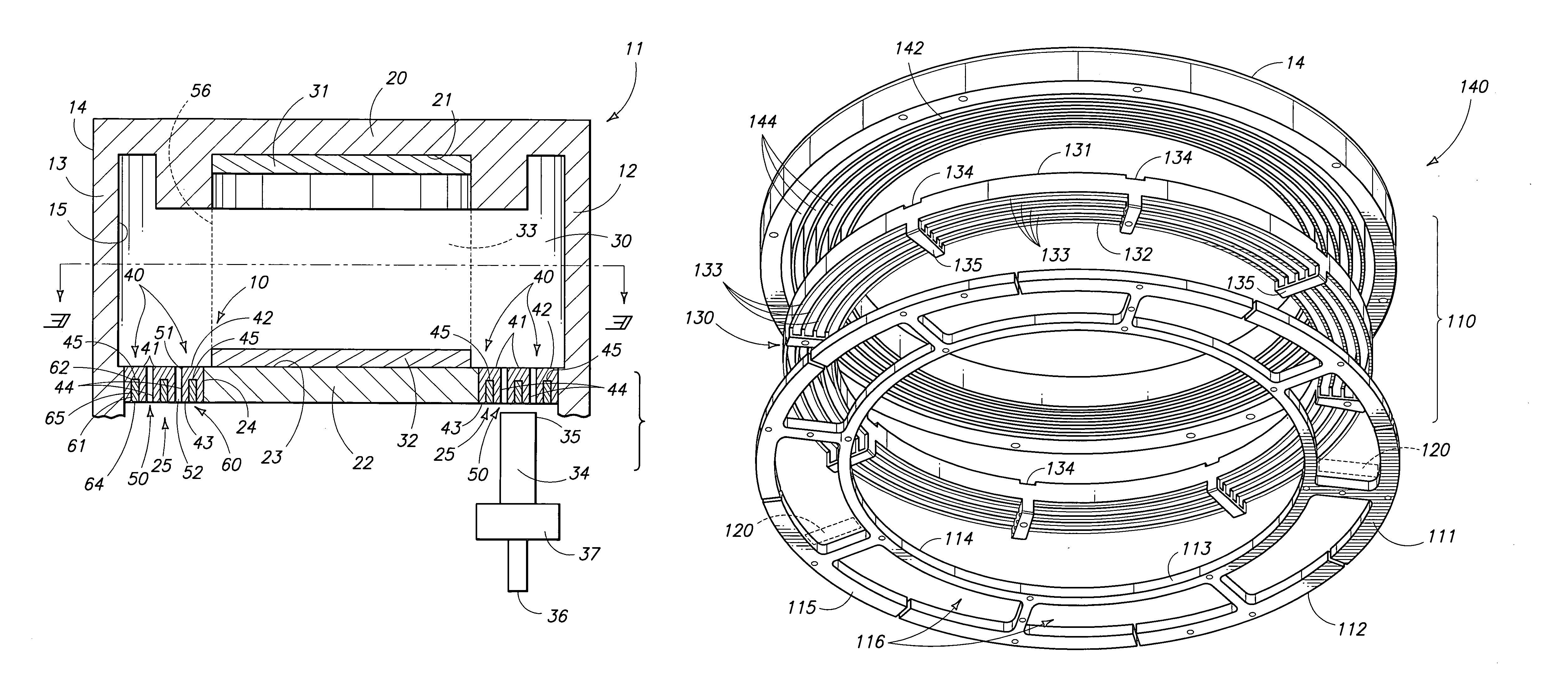
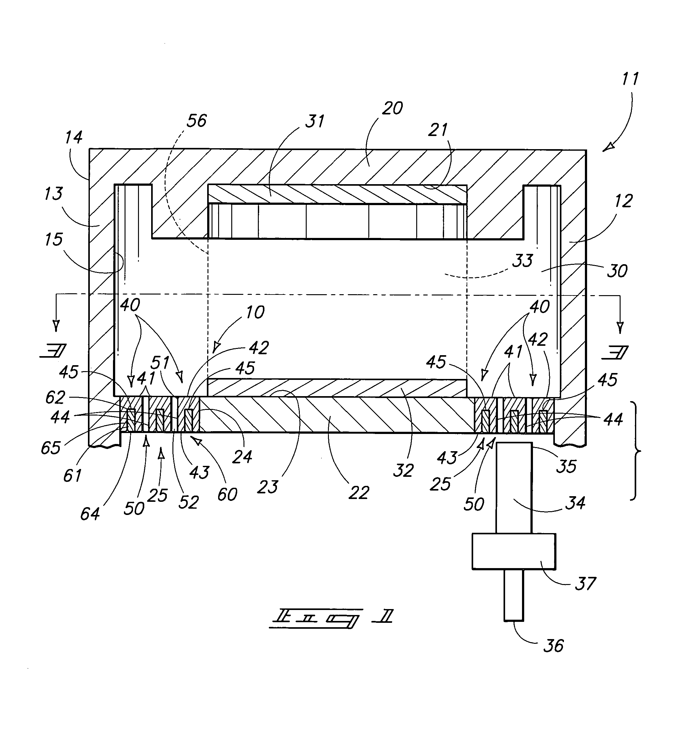
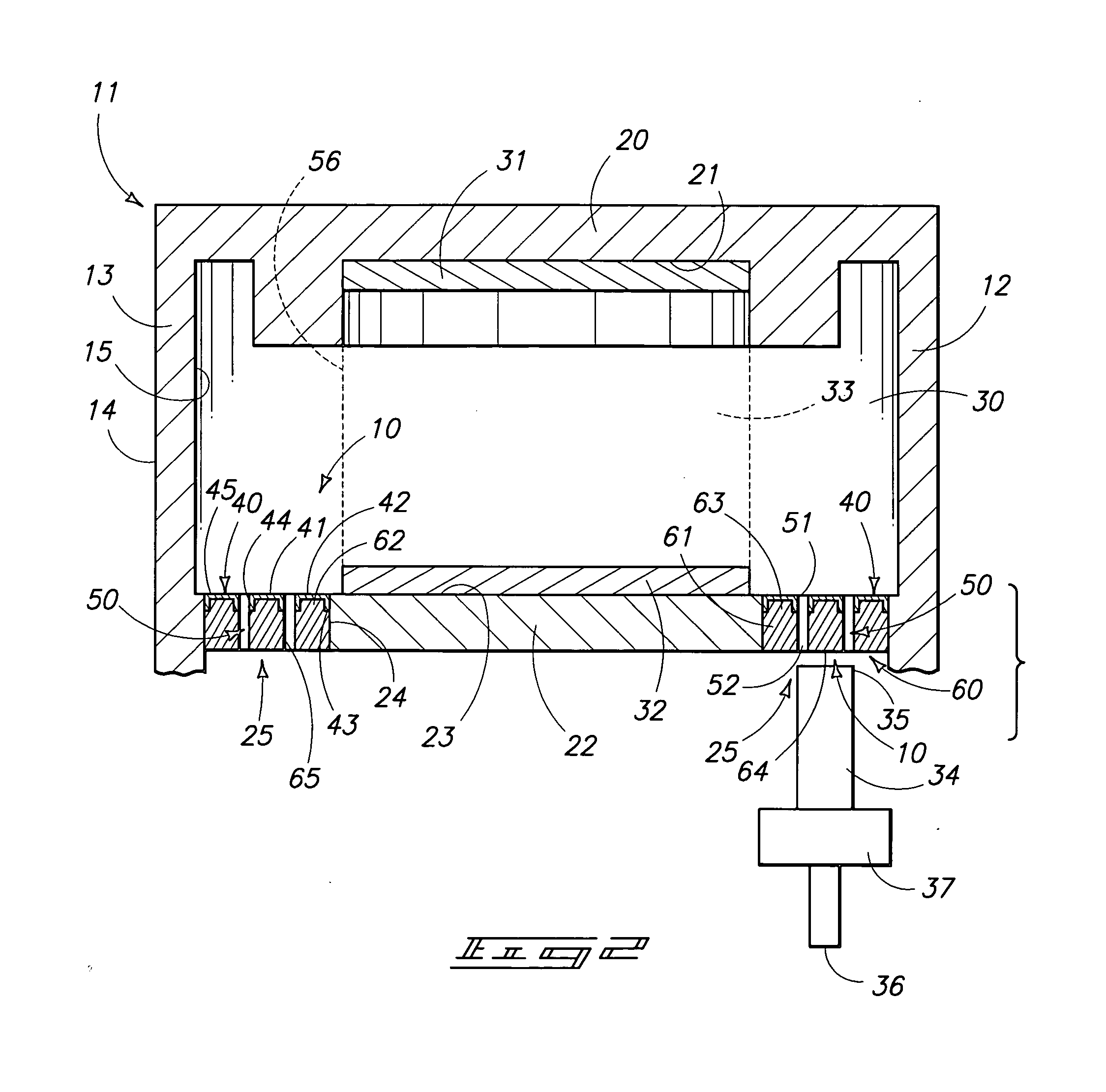
[0029]Referring now to FIG. 1, a first form of the plasma confinement apparatus of the present invention is generally indicated by the numeral 10. The present invention is made integral with a plasma processing apparatus which is generally indicated by the numeral 11. As seen in FIGS. 1-8, the plasma processing apparatus 11 includes a processing chamber which is generally indicated by the numeral 12, and which is defined by a substantially vertically oriented and cylindrically shaped sidewall 13. In one form of the invention, the processing chamber is electrically conductive. The sidewall 13 has an outside facing surface 14, and an opposite inside facing surface 15. Still further, the plasma processing chamber 12 has a top portion 20, which is defined, in part, by an inside facing surface...


PUM

PropertyMeasurementUnit
electrically insulativeaaaaaaaaaa
electrically conductiveaaaaaaaaaa
electricallyaaaaaaaaaa

Abstract

A plasma confinement apparatus, and method for confining a plasma are described and which includes, in one form of the invention, a plurality of electrically insulated components which are disposed in predetermined spaced relation, one relative to the others, and surrounding a processing region of a plasma processing apparatus, and wherein a plurality of passageways are defined between the respective insulated components; and at least one electrically conductive and grounded component forms an electrical field shielding for the processing region.

Description

RELATED PATENT DATA[0001]This application claims priority from Chinese Patent Application Serial Nos. 200510030576.3, which was filed on Oct. 14, 2005, and 200610116449.X and which was filed on Sep. 22, 2006.TECHNICAL FIELD[0002]The present invention relates to a plasma confinement apparatus for use in semiconductor processing, and related method for confining a plasma, and more specifically to an arrangement which provides electrical field shielding for a processing region within a plasma processing apparatus.BACKGROUND OF THE INVENTION[0003]The operation of a plasma processing apparatus, and similar devices in connection with the fabrication of semiconductor substrates or flat panel displays of various types are well known. In this regard, such assemblies include a chamber housing a pair of essentially planar electrodes that are spaced in substantially parallel relation to define a reaction space therebetween. On a first of the electrodes is positioned a semiconductor wafer to be ...

Claims


Application Information

Patent Timeline
Patent Type & Authority Patents(United States)
IPC IPC(8): C23C16/00
CPCC23C16/4404C23C16/5096H01J37/32623H01J37/32642H05H1/03H05H1/26
Inventor NI, TOMCHEN, JINYUANQIAN, QINGFU, YUEHONGXU, ZHAOYANGZHOU, XUSHENGWANG, YE
Owner ADVANCED MICRO FAB EQUIP INC CHINA
Why Eureka
Try Eureka