Method for fabricating monolithic two-dimensional nanostructures

a nanostructure and monolithic technology, applied in nanotechnology, nanoinformatics, semiconductor devices, etc., can solve the problems of difficult to assemble nanowires into desired electrical circuit architectures, nanowires may not be easily accessible using conventional lithographic patterning methods, and nanowire use in electrical applications has several limitations. , to achieve the effect of good gate switching, poor gate modulation, and high quality

Inactive Publication Date: 2014-02-04
CALIFORNIA INST OF TECH
View PDF7 Cites 14 Cited by
  • Summary
  • Abstract
  • Description
  • Claims
  • Application Information

AI Technical Summary

Benefits of technology

[0040]Methods for generating two-dimensional structures at sublithographic dimensions are described below. One dimension may comprise ultra-high density nanowire arrays created by nanowire fabrication processes while the other dimension may comprise lithographically patterned structures or another array of nanowires by nanowire fabrication processes. The fabricated nanowires may be deposited on a layer consisting of a mix of polymethylmethacrylate (PMMA) or other photo-resist material and epoxy, which may serve as both an adhesive for the deposited nanowires and support lithographical patterning. The fabricated two-dimensional structures may then provide structures with reliable electrical contacts to nanowire devices, or structures that allow for the suspension of high density nanowire arrays, structures that provide two-dimensional photonic-like single crystals, or structures having other useful characteristics.
[0042]Doping profile may plan an important role in the performance of nanowire transistors. High doping level favors high quality electrical contacts but yields poor gate modulation while low doping may provide good gate switching, but result in difficulties in forming good contacts. Methods described below incorporate selective etching to form inhomogeneous doping profiles, i.e., high doping in contact regions and low doping in channels. The doping techniques used may result in the dopants residing on the nanowire surfaces. After electrical contacts are formed to the heavily doped nanowires, the surface of the channel may be etched to remove the top layers of atoms. Hence, low doping in the channel region may be achieved while retaining high doping in the contact regions.
[0043]Ultra-high density nanowire arrays may be suspended as active components for elements such as high frequency resonators. When suspended, adjacent nanowires in an array tend to bond to each other due to Van der Walls forces. Methods described below provide for the formation of monolithic bars to hold nanowires in a high density array. The connections may be single crystalline in nature, where the rigidity of the crystal helps clamp nanowires in the array.

Problems solved by technology

Such dimensions may not be readily accessible using conventional lithographic patterning methods, but may be made accessible using nanowire patterning or nanowire materials growth methods.
While nanowires have a number of electronic applications that may not be shared by larger submicrometer or micrometer scale wires, the use of nanowires in electrical applications have several limitations.
First, it may not be easy to assemble nanowires into desired electrical circuit architectures.
Second, establishing electrical contact to nanowires may be difficult.
There is no general approach to establish ohmic electric contacts to nanowires.
As indicated, establishing good electrical contacts between different materials is generally difficult, and is generally more difficult when one of the materials is a nanowire.
However, for nanowires that are lightly doped, as is required for field-effect transistors, chemical sensing, thermoelectric, and other applications, ohmic contacts to the nanowires are much more difficult to achieve.
Typically, such methods are limited to either semiconductor nanowires that are nucleated and grown from a metal nanoparticle seed, or carbon nanotubes that are similarly nucleated and grown.
Arrays of suspended nanowires can have superior signal-to-noise performance over individual nanowires, but may be difficult to suspend because the nanowires themselves can exhibit strong nanowire-nanowire interactions that can cause the structure to collapse.
Nanowires less than 20 nm in width are attractive building blocks for advanced electronic devices, but the small sizes may impose challenges in forming reliable electrical contacts using metal pads due to high surface sensitivity unique to nanowires.
High doping level favors high quality electrical contacts but yields poor gate modulation while low doping may provide good gate switching, but result in difficulties in forming good contacts.
The doping techniques used may result in the dopants residing on the nanowire surfaces.

Method used


Image

  • Method for fabricating monolithic two-dimensional nanostructures
  • Method for fabricating monolithic two-dimensional nanostructures
  • Method for fabricating monolithic two-dimensional nanostructures

Examples


Embodiment Construction

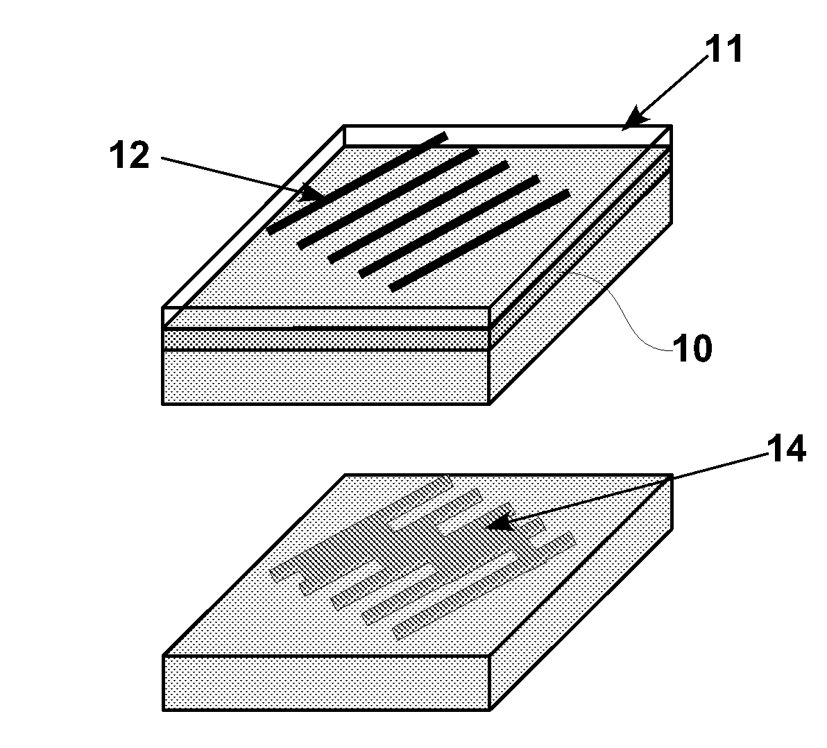
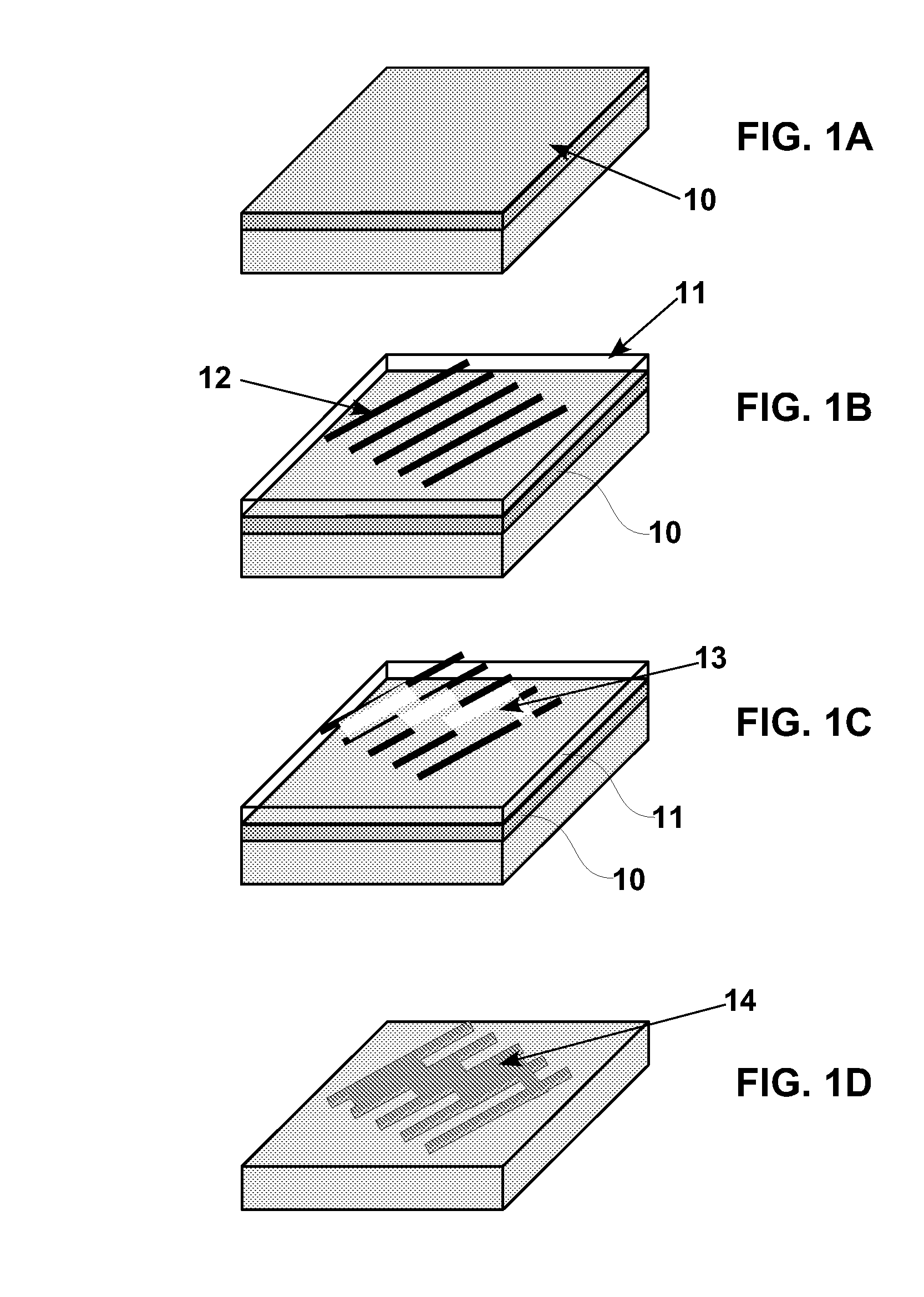
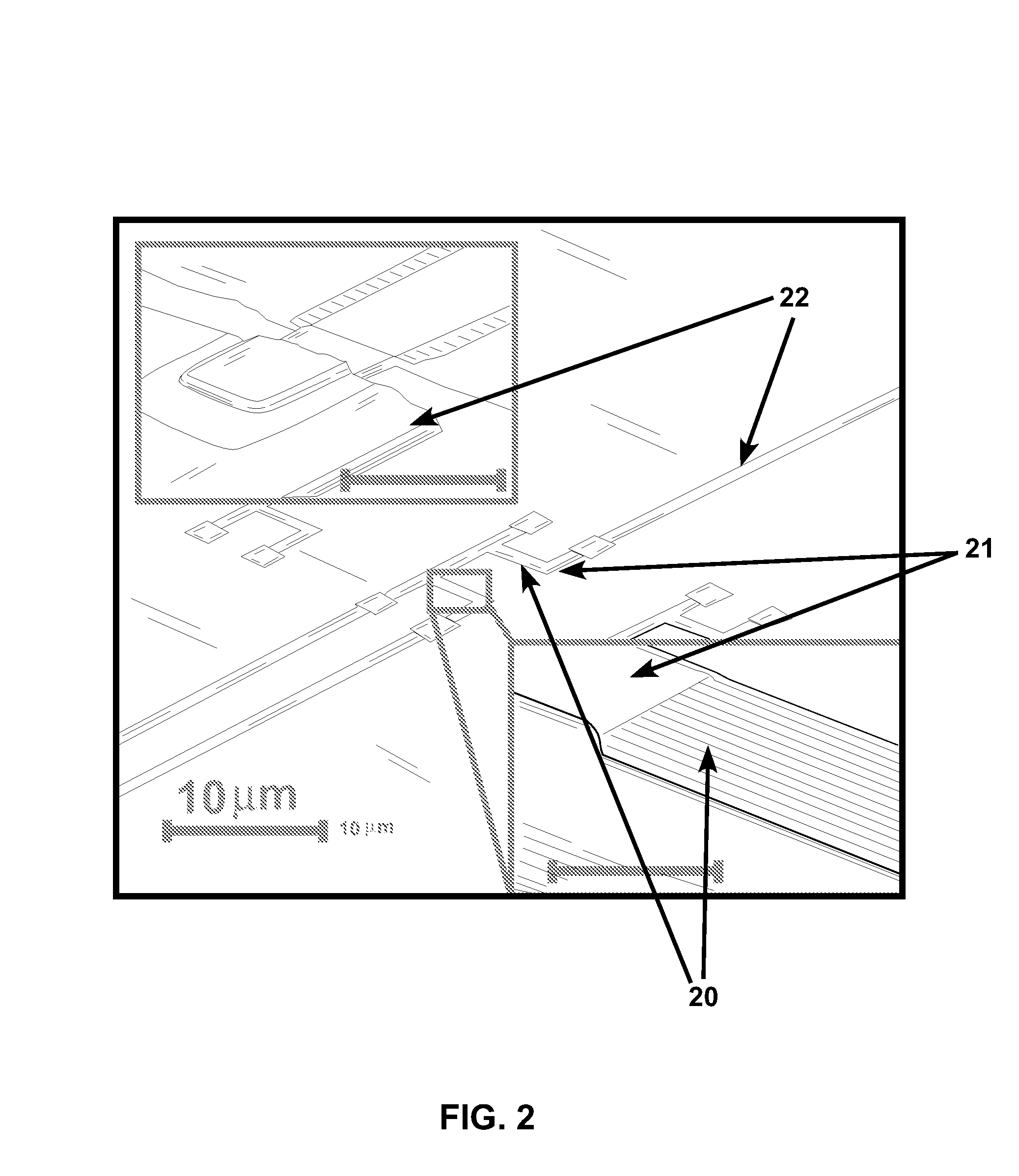
[0059]Nanowire materials, which can exhibit unique and useful properties because of their small dimensions, can typically only be assembled or patterned to form periodic, simple structures. Such simple structures are often inappropriate, not optimal, or not useful for an application of interest. On the other hand, lithographic patterning may be utilized to produce arbitrarily complex patterns, as required by an application of interest. However, lithographic patterning does not resolve the same nanoscale dimensions and nanostructure packing densities that can be achieved using nanowire patterning or assembly methods. As described below, embodiments of the present disclosure provide for the fabrication of structures that can include nanowires with electrical contacts and arbitrarily complex signal routing and interconnect patterns. Embodiments of the present disclosure may also provide that all structures be fabricated from the same material, or even the same single crystal. Embodimen...


PUM

PropertyMeasurementUnit
widthaaaaaaaaaa
angleaaaaaaaaaa
thickaaaaaaaaaa

Abstract

A patterning method for the creation of two-dimensional nanowire structures. Nanowire patterning methods are used with lithographical patterning approaches to form patterns in a layer of epoxy and resist material. These patterns are then transferred to an underlying thin film to produce a two-dimensional structure with desired characteristics.

Description

CROSS-REFERENCE TO RELATED APPLICATIONS[0001]The present application is related to and claims the benefit of commonly assigned U.S. Patent Application No. 60 / 931,432, titled “Fabricating Monolithic Two-Dimensional Si Nanostructures,” filed on May 23, 2007, the entire contents of which are incorporated herein by reference.STATEMENT REGARDING FEDERALLY SPONSORED RESEARCH OR DEVELOPMENT[0002]The U.S. Government has certain rights in this invention pursuant to Grant No. HR0011-04-3-0038 awarded by DARPA.BACKGROUND[0003]1. Field[0004]This disclosure relates to nanowire assembly methods. More specifically, the present disclosure describes methods for nanowire patterning and assembly methods to form circuits and other structures.[0005]2. Description of Related Art[0006]Nanowires are a class of materials in which the diameter or width of the nanowires itself varies from a few nanometers to a few tens of nanometers. Such dimensions may not be readily accessible using conventional lithographi...

Claims


Application Information

Patent Timeline
Patent Type & Authority Patents(United States)
IPC IPC(8): B44C1/22C23F1/00
CPCH01L29/0673B82Y10/00H01L21/0331H01L29/78696H01L29/0665H01L21/3086
Inventor HEATH, JAMES R.WANG, DUNWEIBUNIMOVICH, YURIBOUKAI, AKRAM
Owner CALIFORNIA INST OF TECH
Why Eureka
Try Eureka