Method for improving uniformity of chemical-mechanical planarization process

a chemical-mechanical and process technology, applied in semiconductor devices, semiconductor/solid-state device testing/measurement, electrical equipment, etc., can solve the problems of large gap between silicon oxide and polysilicon gates, the most difficult in the industry, and the inability to effectively eliminate great thickness differences, etc., to achieve the effect of improving the uniformity of the chemical-mechanical planarization process and improving the uniformity of the within-in-di

Active Publication Date: 2014-02-11
INST OF MICROELECTRONICS CHINESE ACAD OF SCI
View PDF8 Cites 104 Cited by
  • Summary
  • Abstract
  • Description
  • Claims
  • Application Information

AI Technical Summary

Benefits of technology

[0007]Thus, the purpose of the invention lies in proposing a method for improving the within-in-die uniformity, and in particular effectively improving the uniformity of the subsequent metal gate CMP for the POP CMP process.
[0008]The invention provides a method for improving uniformity of chemical-mechanical planarization process, comprising the steps of: forming features on a substrate; forming a first dielectric isolation layer between the features; planarizing the first dielectric isolation layer until the features are exposed, causing the first dielectric isolation layer between the features to have a recess depth; forming a second dielectric isolation layer on the features and the first dielectric isolation layer, at least refilling the recess of dielectric isolation layer caused by the first chemical-mechanical planarization, whereby reducing the difference in is height between the second dielectric isolation layer between the features and the second dielectric isolation layer on the top of the features; and planarizing the second dielectric isolation layer until the features are exposed.
[0015]According to the method for improving uniformity of chemical-mechanical planarization process of the invention, a dielectric isolation layer is formed again after grinding the dielectric isolation layer on the top of the features, such that the difference in height between the dielectric layer between the features and the dielectric layer on the top of the features is effectively reduced, and the recess of the dielectric layer between the features is compensated, hence, the within-in-die uniformity is effectively improved.

Problems solved by technology

The development of the chemical-mechanical planarization (CMP) process in the gate-last process integration is regarded to be the most challenging in the industry.
As technology nodes continuously decrease in size, the conventional CMP meet with extremely high challenge in terms of improving the within-in-die uniformity for technology nodes below 45 nm.
If the conventional silicon oxide CMP process is employed, such great thickness differences cannot be effectively eliminated, which will be kept with the implementation of the polishing procedure until the silicon oxide polishing ends, causing large to recess to exist in the silicon oxide between polysilicon gates.
Even the next step silicon nitride CMP hardly can repair it, and due to the difference in material selectivity, such silicon oxide recess may be further enlarged, as shown in FIG. 1B, the silicon oxide between gates has a first recess depth H1 which is, e.g., about 100 Å. A large recess of the silicon oxide layer 4 will directly cause a great obstacle to the metal gate CMP process, it will drastically limit the tuning range of the process.
Likewise, as far as other features which demand for the planarization processing are concerned, such as the fin structure, the multi-gate structure, the MEMS structure and etc., they also have the similar problem, the recess of the dielectric isolation layer between the features will be kept and enlarged in the subsequent processing course, resulting in failure of the features.

Method used


Image

  • Method for improving uniformity of chemical-mechanical planarization process
  • Method for improving uniformity of chemical-mechanical planarization process
  • Method for improving uniformity of chemical-mechanical planarization process

Examples


Embodiment Construction

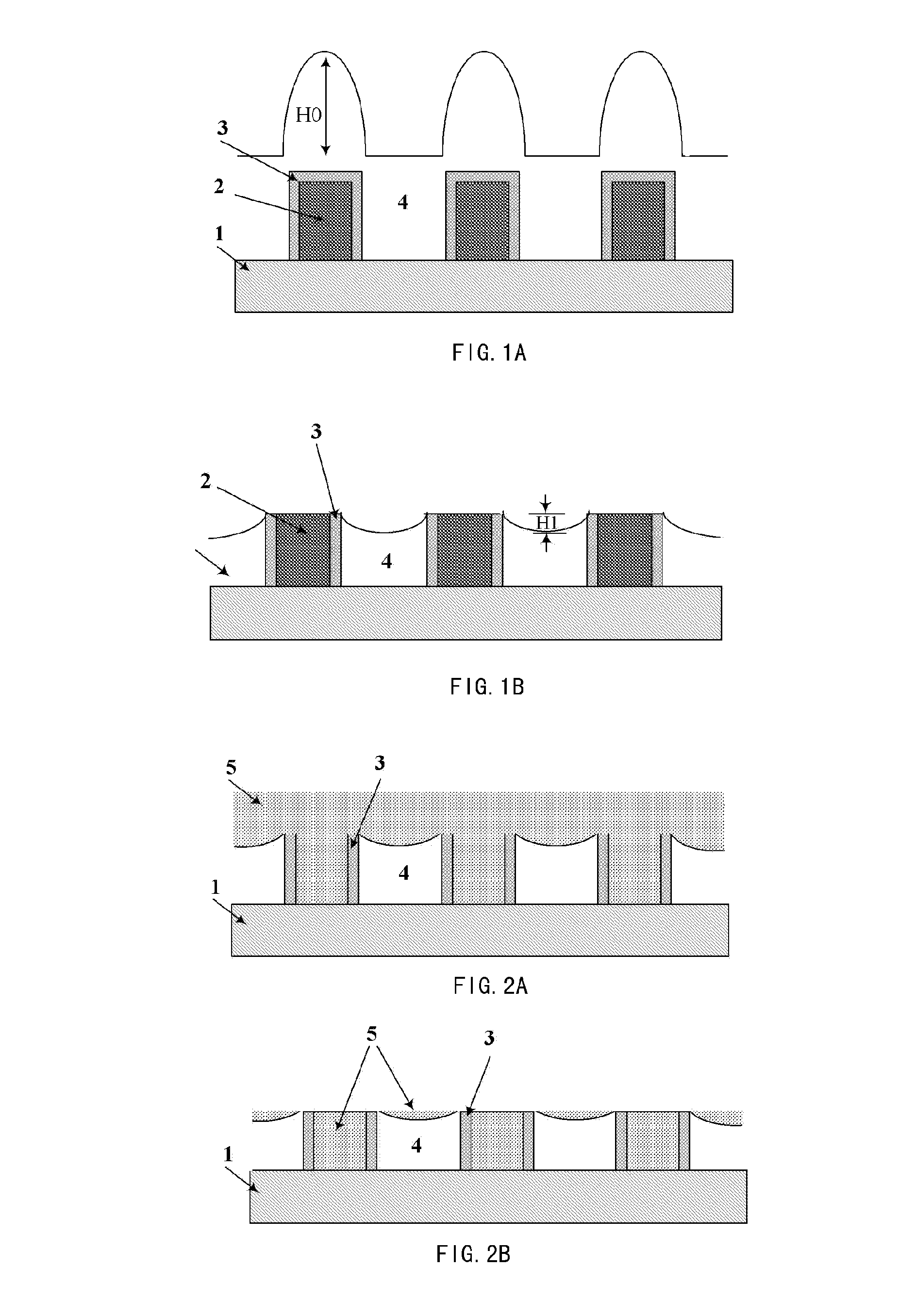
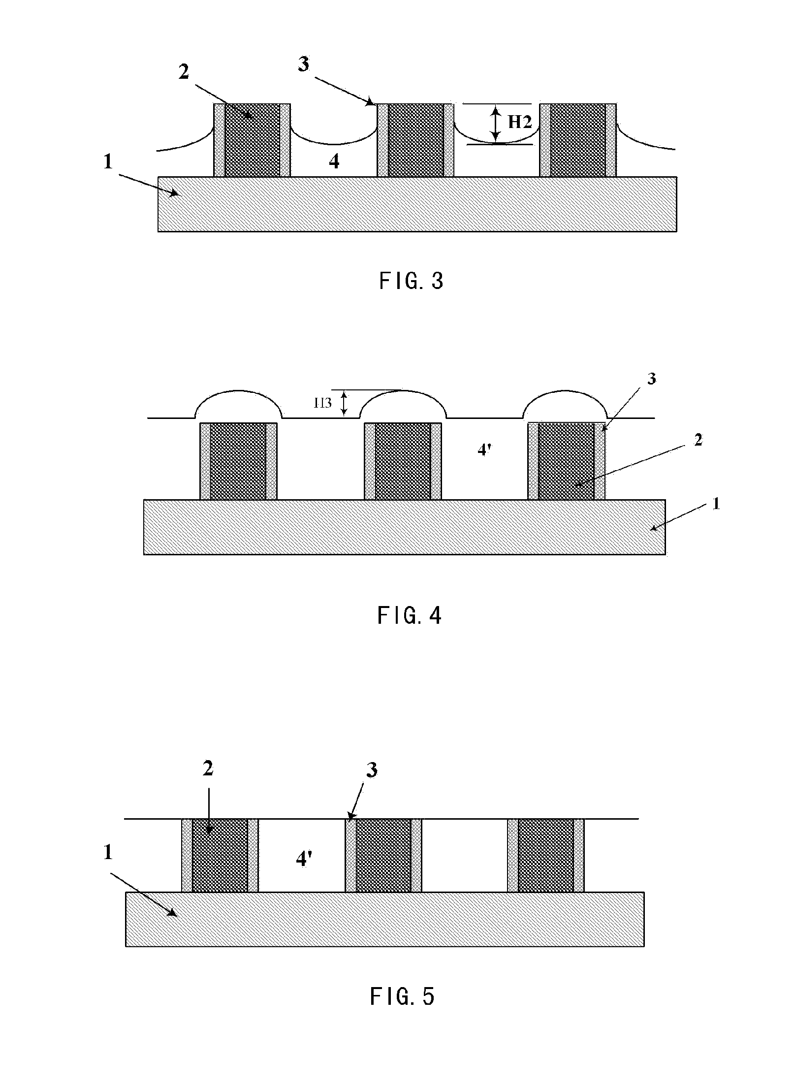
[0020]In the following text, the features and technical effects of the technical solution of the invention are expounded with reference to the Figures in combination with the illustrative embodiments, and the method for improving the uniformity of chemical-mechanical planarization process is disclosed. It needs to be pointed out that similar reference signs represent similar structures.

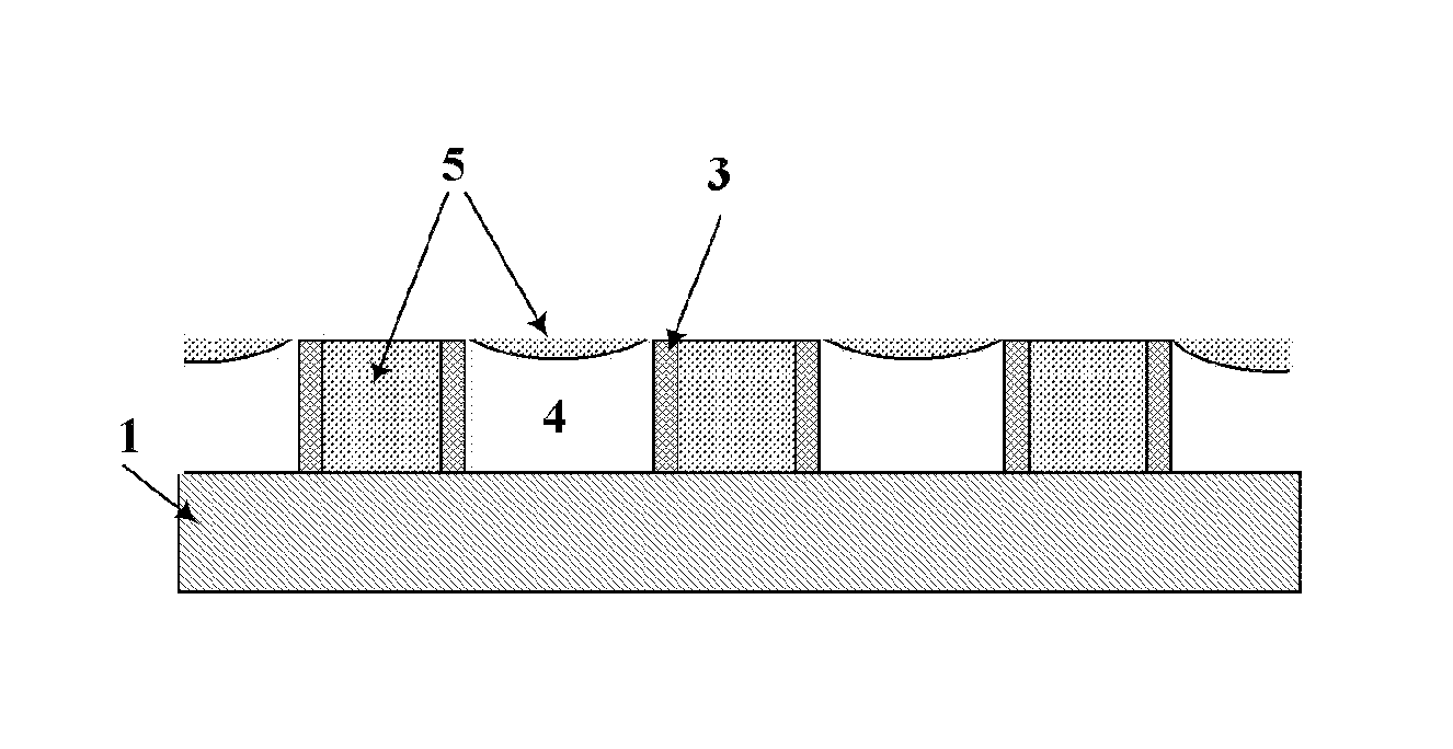
[0021]In the POP CMP process, the recess of a dielectric isolation layer formed of, e.g., silicon oxide, which is generated between the features of, e.g., polysilicon gates, substantively is caused by the height difference between the structure and the portion between the features, e.g., source / drain regions; that is, after a dielectric isolation layer is grown, the dielectric isolation layer on the top of the features is higher than that between the features, which is unfavorable to the control of the recess of the dielectric isolation layer between the features in the CMP process. The designing idea...


PUM


Abstract

The invention provides a method for improving uniformity of chemical-mechanical planarization process, comprising the steps of: forming features on a substrate; forming a first dielectric isolation layer between the features; planarizing the first dielectric isolation layer until the features are exposed, causing the first dielectric isolation layer between the features to have a recess depth; forming a second dielectric isolation layer on the features and the first dielectric isolation layer, whereby reducing the difference in height between the second dielectric isolation layer between the features and the second dielectric isolation layer on the top of the features; planarizing the second dielectric isolation layer until the features are exposed. According to the method for improving uniformity of chemical-mechanical planarization process of the invention, a dielectric isolation layer is formed again after grinding the dielectric isolation layer on the top of the features, such that the difference in height between the dielectric layer between the features and the dielectric layer on the top of the features is effectively reduced, and the recess of the features is compensated, the within-in-die uniformity is effectively improved.

Description

CROSS REFERENCE[0001]This application is a National Phase application of, and claims priority to, PCT Application No. PCT / CN2012 / 000802, filed on Jun. 12, 2012, entitled “A Method for improving Uniformity of Chemical-Mechanical Planarization Process'”, which claimed priority to Chinese Application No. CN 201210112494.3, filed on Apr. 16, 2012. Both the PCT Application and Chinese Application are incorporated herein by reference in their entireties.FIELD OF THE INVENTION[0002]The invention relates to a manufacturing method of semiconductor devices, and more specifically, relates to a method for improving uniformity of chemical-mechanical planarization process.BACKGROUND OF THE INVENTION[0003]The successful application of high-K / metal gate engineering on the 45 nm technology node has made it essential and key modular engineering for technology nodes below sub-30 nm. The high-K / metal gate is divided into gate-first process and gate-last process. Since the gate-last process avoids the n...

Claims


Application Information

Patent Timeline
Patent Type & Authority Patents(United States)
IPC IPC(8): H01L21/461H01L21/302H01L21/311
CPCH01L21/31053H01L21/30625H01L22/26H01L21/31056H01L2924/0002H01L29/66545H01L2924/00
Inventor YANG, TAOZHAO, CHAOLI, JUNFENG
Owner INST OF MICROELECTRONICS CHINESE ACAD OF SCI
Why Eureka
Try Eureka