
Analog to digital converter circuit

a converter circuit and analog-to-digital converter technology, applied in analogue/digital conversion, transmission systems, instruments, etc., can solve the problems of flash adc being the fastest, having the highest implementation cost, and sar adc being considerably slower than flash adc, so as to improve the feedback factor

Active Publication Date: 2014-02-25
UNIVERSITY OF MACAU
View PDF1 Cites 40 Cited by
  • Summary
  • Abstract
  • Description
  • Claims
  • Application Information

AI Technical Summary

Benefits of technology

The present invention provides a power-efficient and high-speed analog-to-digital converter (ADC) circuit. It includes multiple time-interleaved pipelined-successive approximation register (SAR) ADCs, which use a residue amplifier and a digital error correction logic to combine the digital codes generated by two stages of SAR sub-ADCs to produce a high-quality digital signal that represents the analog input signal. The first stage SAR sub-ADC uses a flip-around Multiplying Digital to Analog Converter (MDAC) to improve feedback factor. This design consumes less power than many other ADCs and achieves high-speed performance.

Problems solved by technology

Flash ADC is typically the fastest, but has the highest implementation cost.
SAR ADC has a much lower implementation cost, however, it is considerably slower than flash ADC.
As to the pipelined ADC, it does not benefit from the technology scaling because the use of low voltage supplies gives rise to an augmented consumption of power.

Method used


Image

  • Analog to digital converter circuit
  • Analog to digital converter circuit
  • Analog to digital converter circuit

Examples


Embodiment Construction

[0020]In the following description of preferred embodiments, reference is made to the accompanying drawings which form a part hereof, and in which it is shown by way of illustration specific embodiments in which the invention can be practiced. It is to be understood that other embodiments can be used and structural changes can be made without departing from the scope of the embodiments of this invention.

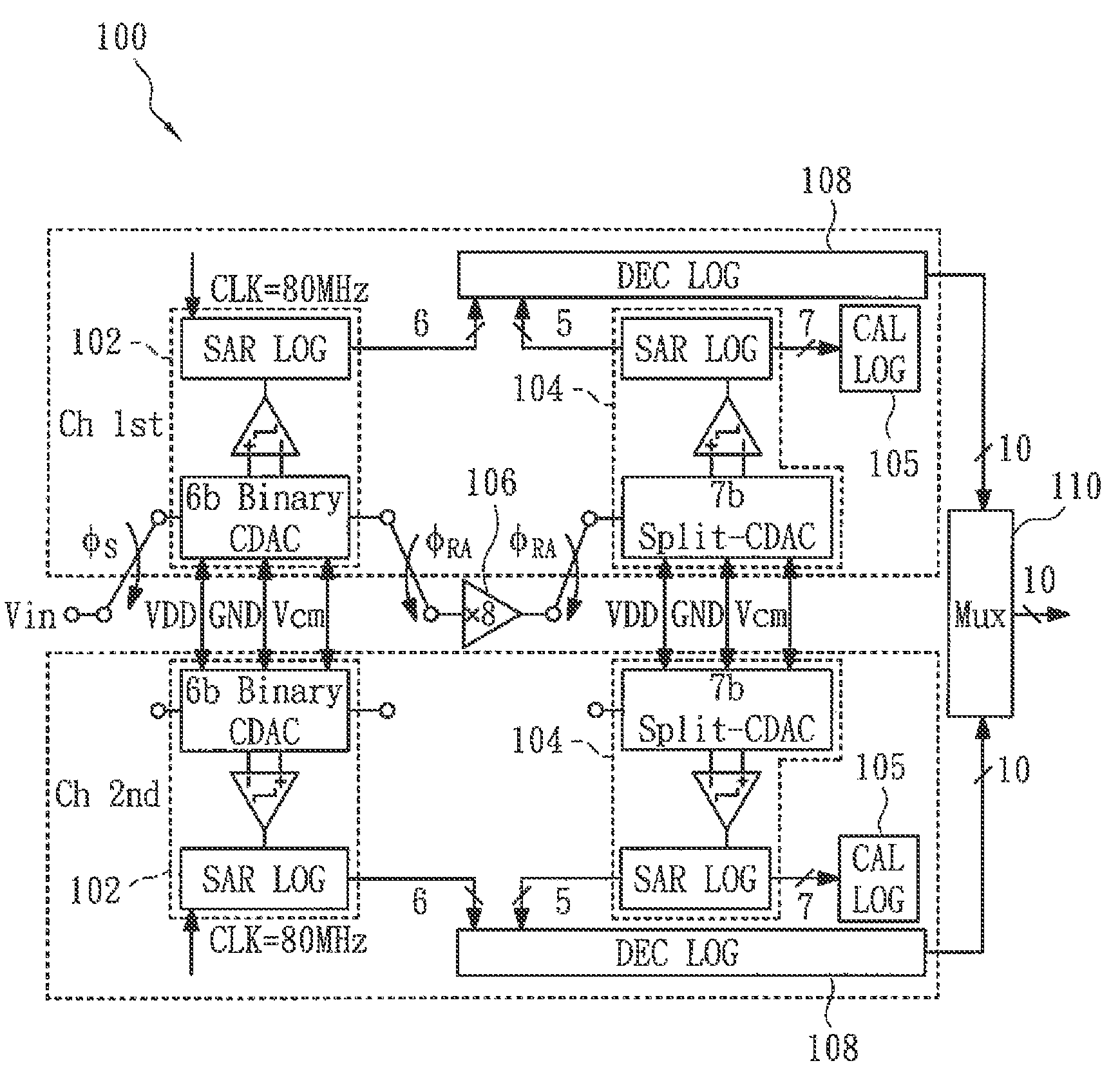
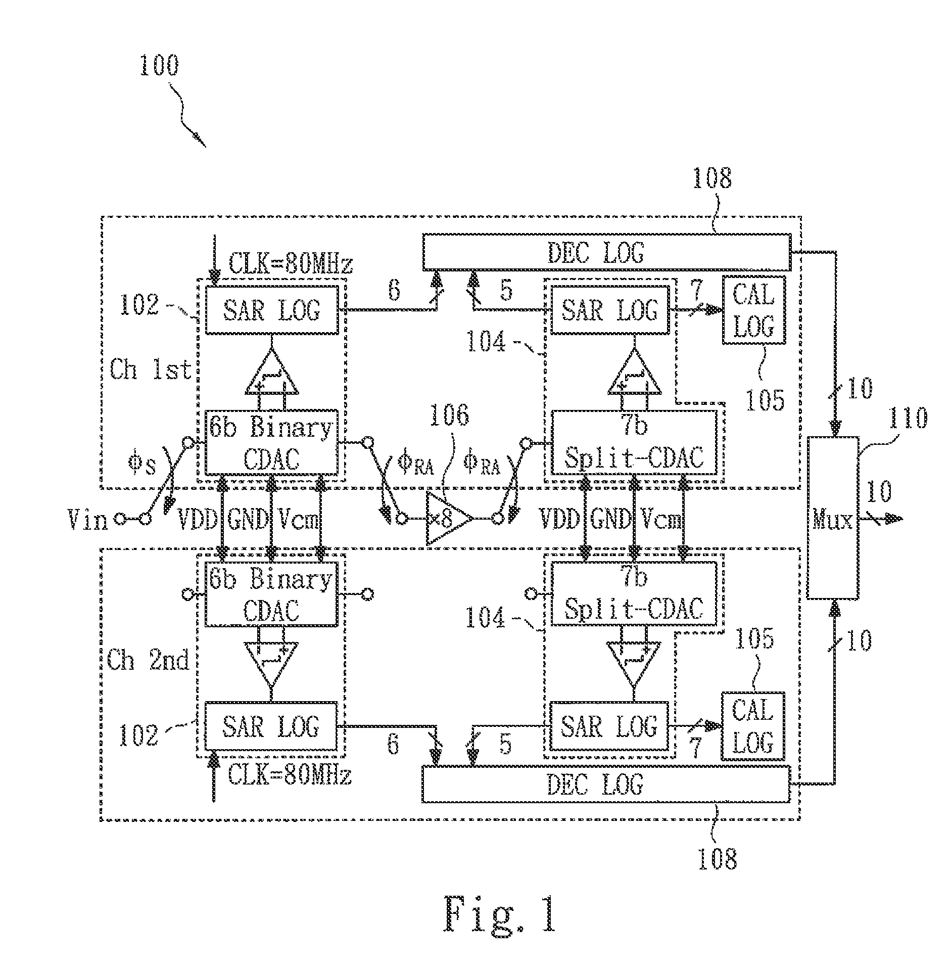
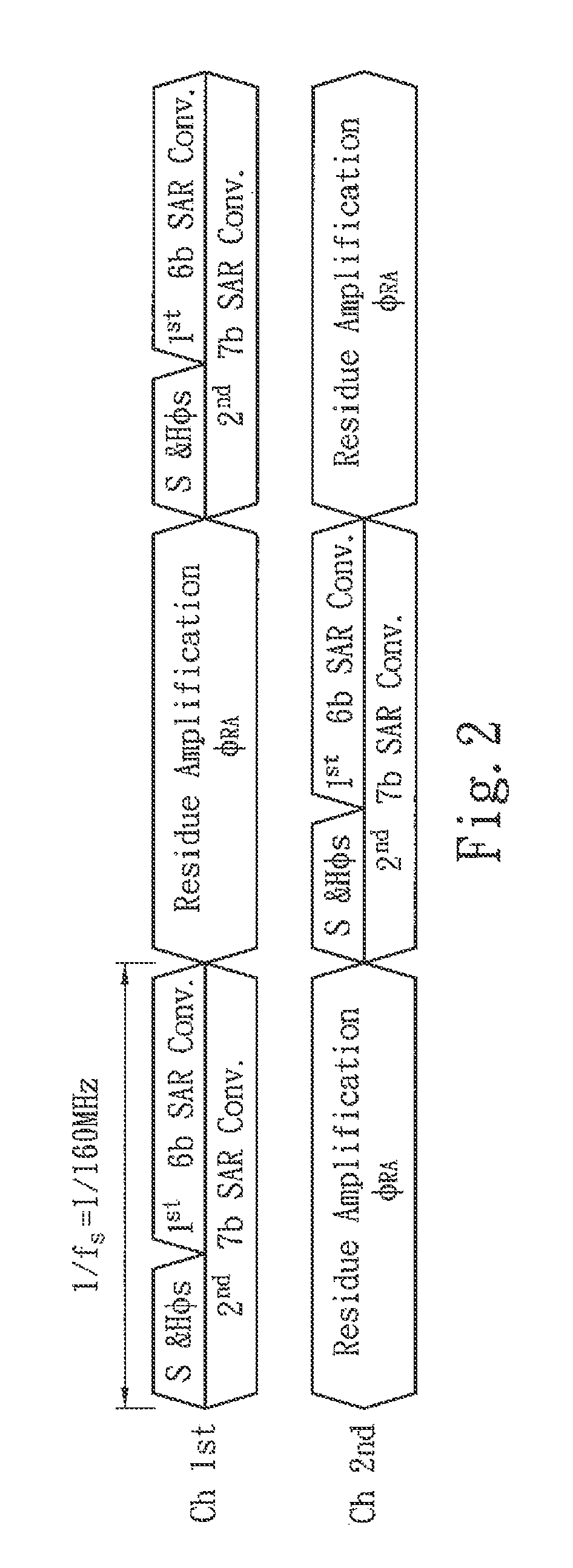
[0021]Reference is now made to FIG. 1. FIG. 1 is a block diagram of an analog to digital converter (ADC) according to an embodiment of the present invention. A time-interleaved successive approximation register (SAR) ADC circuit 100 with 10-bit resolution and 160 MS / s sampling rate is shown in FIG. 1. The ADC circuit 100 includes two interleaved pipelined-SAR ADCs. Each of the SAR ADCs comprises a first stage SAR sub-ADC 102, a second stage SAR sub-ADC 104, a residue amplifier 106 and a digital error correction logic 108. FIG. 2 is a timing diagram illustrating the time relationship ...


PUM


Abstract

The present invention provides a pipelined-successive approximation register (SAR) analog-to-digital converter (ADC) circuit with decoupled flip-around MDAC, capacitive attenuation solution and self-embedded offset cancellation. The flip-around MDAC architecture is built for low inter-stage gain implementation. A capacitive attenuation solution is provided for minimizing the power dissipation and optimizing conversion speed. The design reuses SAR ADC to perform offset cancellation, which significantly saves calibration area, power and time.

Description

FIELD OF THE INVENTION[0001]The present invention relates to an analog to digital converter (ADC), and more particularly, to the time-interleaved pipelined successive approximation register (SAR) ADCs.RELATED ART[0002]Typically, an analog-to-digital converter (ADC) is used for converting an input analog voltage (or current) to a digital number proportional to the magnitude of the voltage or current.[0003]Analog-to-digital converter (ADC) has various architectures, for example, flash analog-to-digital converters (flash ADC), pipeline analog-to-digital converters (pipeline ADC), and successive approximation register analog-to-digital converters (SAR ADC), all of which has respective application field.[0004]Flash ADC is typically the fastest, but has the highest implementation cost. SAR ADC has a much lower implementation cost, however, it is considerably slower than flash ADC. As to the pipelined ADC, it does not benefit from the technology scaling because the use of low voltage suppl...

Claims


Application Information

Patent Timeline
IPC IPC(8): H03M1/12
CPCH03M1/468H03M1/12H03M1/164H03M1/1019H03M1/804H03M1/0695H03M1/1215
Inventor ZHU, YANCHAN, CHI-HANGSIN, SAI-WENGU, SENG-PANSILVA MARTINS, RUI PAULO DAMALOBERTI, FRANCO
Owner UNIVERSITY OF MACAU
Learn More