

Method of fabricating a fast programmable flash E2PROM cell
- Summary
- Abstract
- Description
- Claims
- Application Information
AI Technical Summary
Benefits of technology
Problems solved by technology
Method used
Image

Examples
Embodiment Construction
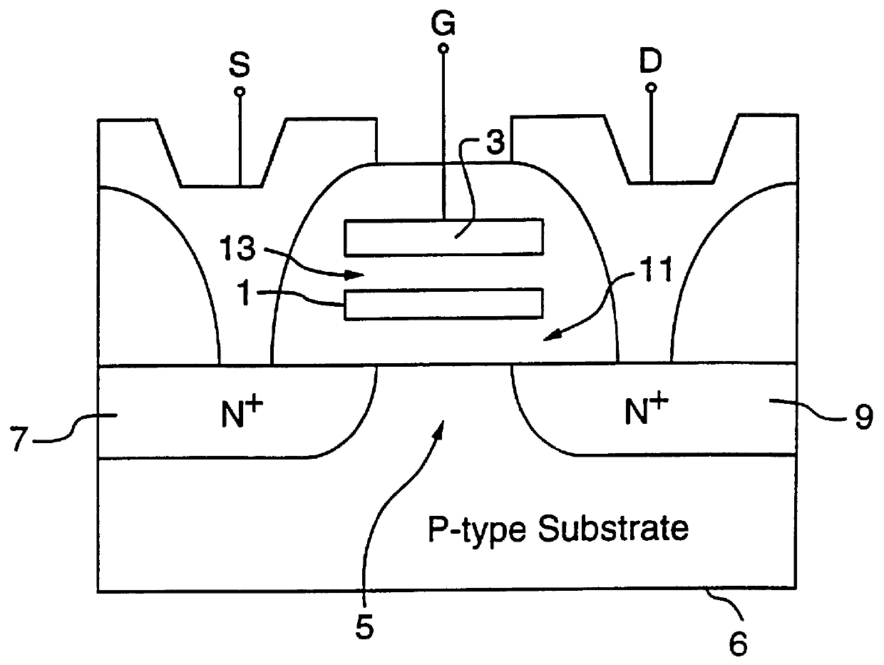
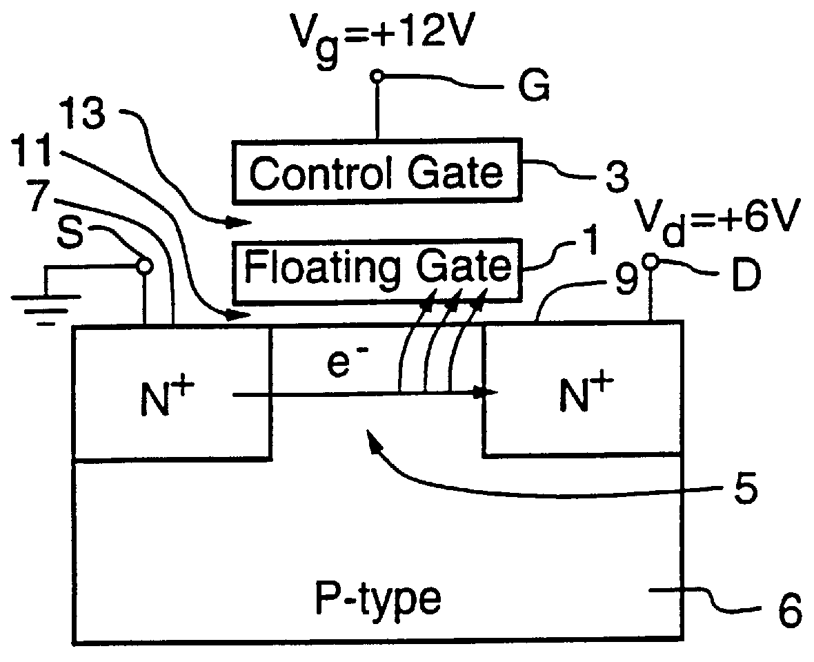
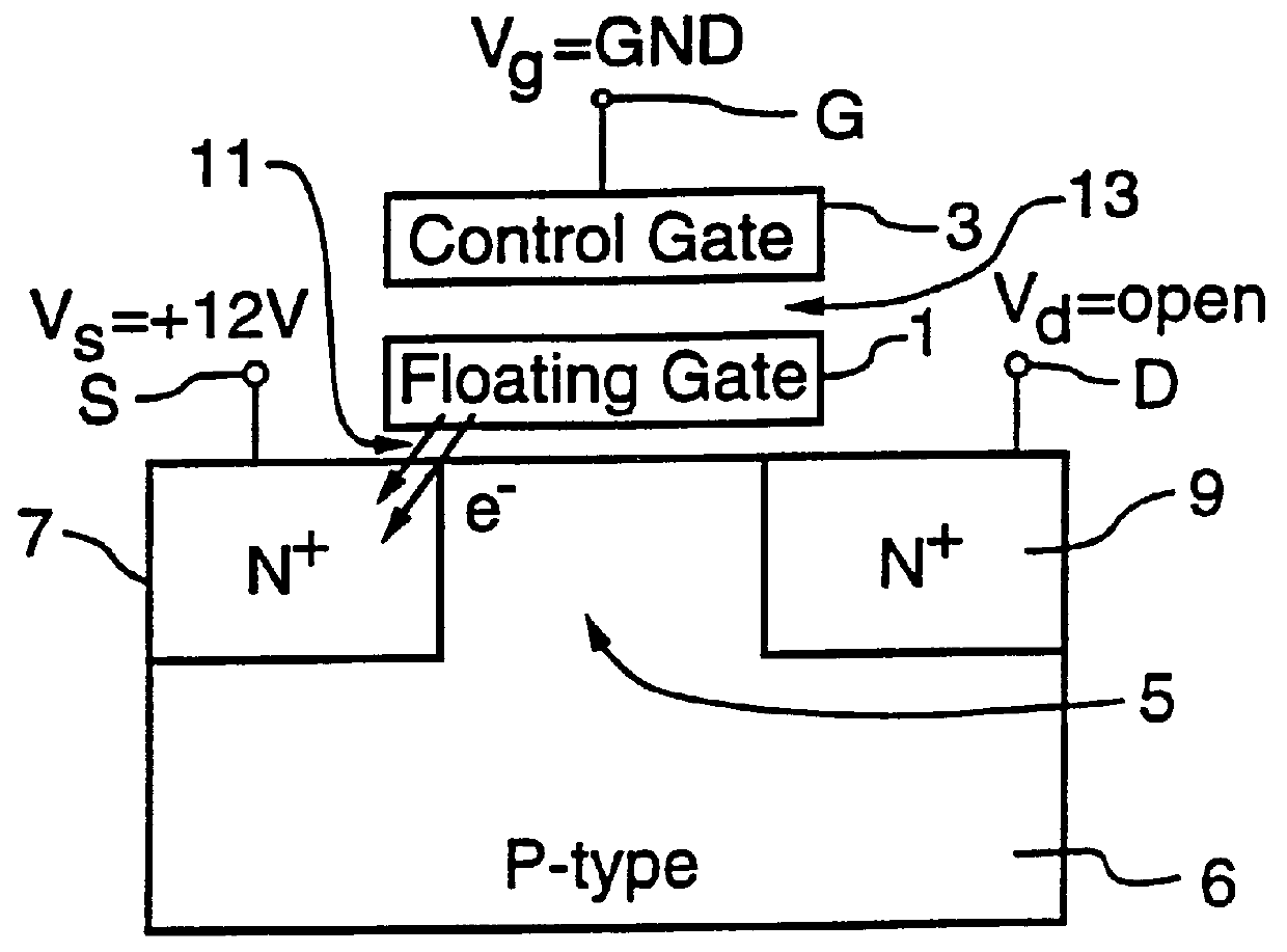
.sup.2 PROM CELL
Turning now to FIG. 5, a flash E.sup.2 PROM cell is shown for achieving simultaneous reduction of programming time and operating voltages over the prior art cell of FIG. 1.
The cell according to the present invention comprises a substrate 15, drain and source regions 17 and 19, respectively, a floating gate 21 and control gate 23, in the usual manner. Tunnel and inter-poly dielectric layers 22 and 24 are also provided in the usual manner. However, in contrast with the prior art ETOX.TM. flash memory cell, additional highly doped regions 25 and 27 are provided adjoining the drain and / or source regions 17 and / or 19, respectively. The additional highly doped regions 25 and 27 (occasionally referred to herein as pocket implants) extend along a portion of the width of the cell structure identified as the program section 29, the remaining sense section 31 being provided for the read operation of the cell, as discussed in greater detail below.
In the illustrated embodiment, t...
PUM
 Abstract
Description
Claims
Application Information