Gallium-nitride-on-diamond wafers and devices, and methods of manufacture

a technology of diamond wafers and diamonds, which is applied in the direction of polycrystalline material growth, crystal growth process, chemically reactive gas, etc., can solve the problems of unacceptably high bow and reduce the thermal resistance of any electronic and optoelectronic device, so as to improve the quality of the epilayer, improve the thermal resistance, and improve the effect of gan-on-diamond wafers

Active Publication Date: 2014-03-18
GROUP4 LABS
View PDF6 Cites 15 Cited by
  • Summary
  • Abstract
  • Description
  • Claims
  • Application Information

AI Technical Summary

Benefits of technology

[0011](1) In the epilayer transfer process for producing GaN-on-diamond engineered wafers described in the parent application, further improvements to the structure and the method are needed to further reduce the thermal resistance of any electronic and optoelectronic devices.
[0015]There is a clear need in the industry for a low-thermal-resistance AlGaN / GaN-on-diamond wafers that have low bow and exhibit contact between the front and the back of the wafer but allow for processing of the wafers using standard techniques. The preferred embodiments disclosed in this application enable device manufacturing and design improvements that dramatically lower the thermal resistance of any AlGaN / GaN HEMT on new substrates, provide significantly lower bow of the wafers and contact between the front and the back without making thru holes in the wafer.Terminology:
[0027]The objective of the present invention is to improve GaN-on-diamond wafers to reach (a) lower thermal resistance and improved epilayer quality, (b) reduce and meet the wafer bow specifications set by commercial foundries, and (c) disclose wafer structures with vias that allow top to bottom electrical connections without having to processes wafers with thru holes, thereby enabling the use of microstrip transmission lines.

Problems solved by technology

(1) In the epilayer transfer process for producing GaN-on-diamond engineered wafers described in the parent application, further improvements to the structure and the method are needed to further reduce the thermal resistance of any electronic and optoelectronic devices.
(2) Improvement of the epilayer quality of final devices realized by the processes disclosed in the parent application.
(3) Wafers have to be flat. The wafer bow is the difference between the maximum and minimum height of any point on a wafer when it is laid on a flat surface as shown in FIG. 12 and the height is measured in a direction perpendicular to the flat surface. The typical requirement for commercial foundry using a stepper is that the wafer bow one a 100 mm wafer has to be around 20 um or less. This thickness is primarily determined by the time of growth and cost of the wafers. CVD diamond grows with intrinsic strain resulting in unacceptably high bow. For this reason, the mentioned commercial bow specification is very difficult to meet for wafers with diameters greater than 25 mm. It is of critical importance for commercial viability to control the GaN-on-diamond wafer bow and met the specification.

Method used


Image

  • Gallium-nitride-on-diamond wafers and devices, and methods of manufacture
  • Gallium-nitride-on-diamond wafers and devices, and methods of manufacture
  • Gallium-nitride-on-diamond wafers and devices, and methods of manufacture

Examples


process embodiment

Detailed Wafer Structure and Process Embodiment Descriptions

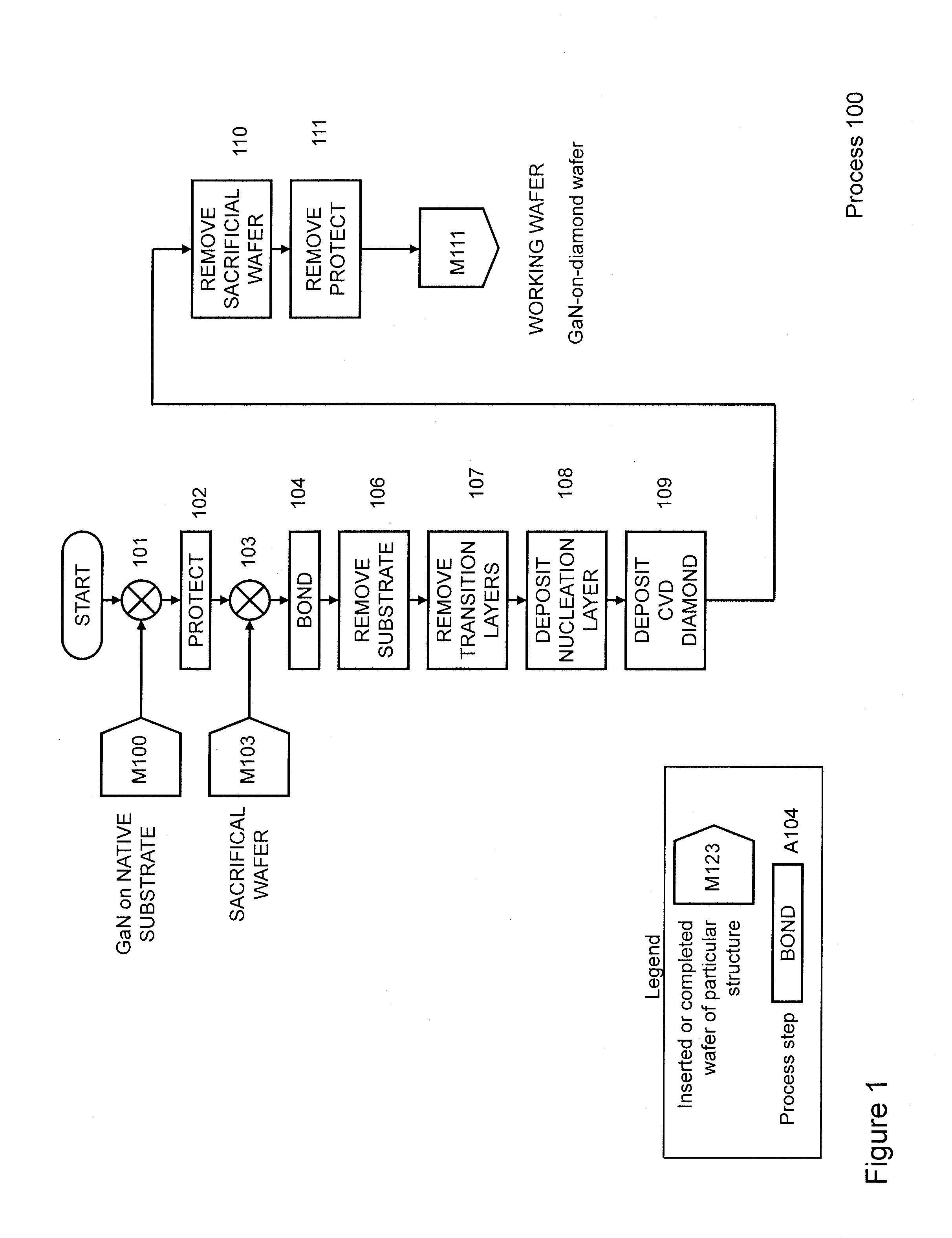
[0107](a) 100-400-500. In one embodiment of preferred method for the manufacturing of high-quality GaN-on-diamond wafers and devices, an as-grown wafer M100 with preferred structure 700 is provided as input to the preferred method 100. The structure of the wafer resulting from process 100 may be, but is not limited to preferred wafer structure 750. The working wafer M111 resulting from process 100 is then provided as input wafer M400 to process 400. The structure of the wafer resulting from process 400 may be, but is not limited to preferred wafer structure 770. In another embodiment, the resulting composite wafer M405 is further processed into devices using process 500, resulting in chips M506 which may have, but are not limited to chip or wafer structure 780.

[0108](b) 100-600. In one embodiment of preferred method for the manufacturing of high-quality GaN-on-diamond wafers and devices, an as-grown wafer M100 with preferre...


PUM

PropertyMeasurementUnit
thicknessaaaaaaaaaa
thicknessaaaaaaaaaa
thicknessaaaaaaaaaa

Abstract

Methods for integrating wide-gap semiconductors, and specifically, gallium nitride epilayers with synthetic diamond substrates are disclosed. Diamond substrates are created by depositing synthetic diamond onto a nucleating layer deposited or formed on a layered structure that comprises at least one layer made out of gallium nitride. Methods for manufacturing GaN-on-diamond wafers with low bow and high crystalline quality are disclosed along with preferred choices for manufacturing GaN-on-diamond wafers and chips tailored to specific applications.

Description

[0001]This application claims the benefit of U.S. Provisional Patent Application Ser. No. 61 / 447,569 filed Feb. 28, 2011, and is a continuation-in-part of (a) U.S. patent application Ser. No. 12 / 484,098 filed Jun. 12, 2009, now U.S. Pat. No. 8,283,672 which is a continuation of U.S. patent application Ser. No. 11 / 279,553 filed Apr. 12, 2006 (now U.S. Pat. No. 7,595,507) and (b) U.S. patent application Ser. No. 12 / 569,486 filed Sep. 29, 2009, now U.S. Pat. No. 8,283,189 which is a divisional of U.S. patent application Ser. No. 11 / 279,553 filed Apr. 12, 2006 (now U.S. Pat. No. 7,595,507), which claims priority from U.S. Provisional Patent Application Ser. No. 60 / 671,411 filed Apr. 13, 2005, and the disclosures of these applications are incorporated herein by reference.FIELD OF THE INVENTION[0002]The present invention relates to high-power electronic and optoelectronic devices and their thermal management, and particularly relates to methods for fabricating such devices and structures ...

Claims


Application Information

Patent Timeline
Patent Type & Authority Patents(United States)
IPC IPC(8): H01L23/532H01L29/20
CPCC30B7/005H01L29/66462H01L21/02488H01L23/3732H01L21/02444H01L29/2003H01L21/02447H01L21/02491H01L21/76838H01L29/7787H01L21/02376H01L21/02502H01L21/02381H01L21/78H01L29/1602H01L21/02458H01L21/02527H01L21/0254H01L21/0405H01L21/0262C30B25/183C30B29/406H01L24/32H01L2924/12032H01L2924/12041H01L2924/1305H01L2924/12042
Inventor BABI, DUBRAVKOFAILI, FIROOZFRANCIS, DANIELDIDUCK, QUENTINEJECKAM, FELIX
Owner GROUP4 LABS
Why Eureka
Try Eureka