

Power amplifier with tunable bandpass and notch filter
a power amplifier and bandpass technology, applied in the direction of transmission, electrical equipment, etc., can solve the problems of rf transmit linearity, rf receive signal, rf transmit signal integration, noise, power consumption requirements, etc., to reduce rf signal swing, reduce rf receive band noise, and reduce noise spur
- Summary
- Abstract
- Description
- Claims
- Application Information
AI Technical Summary
Benefits of technology
Problems solved by technology
Method used
Image

Examples
Embodiment Construction
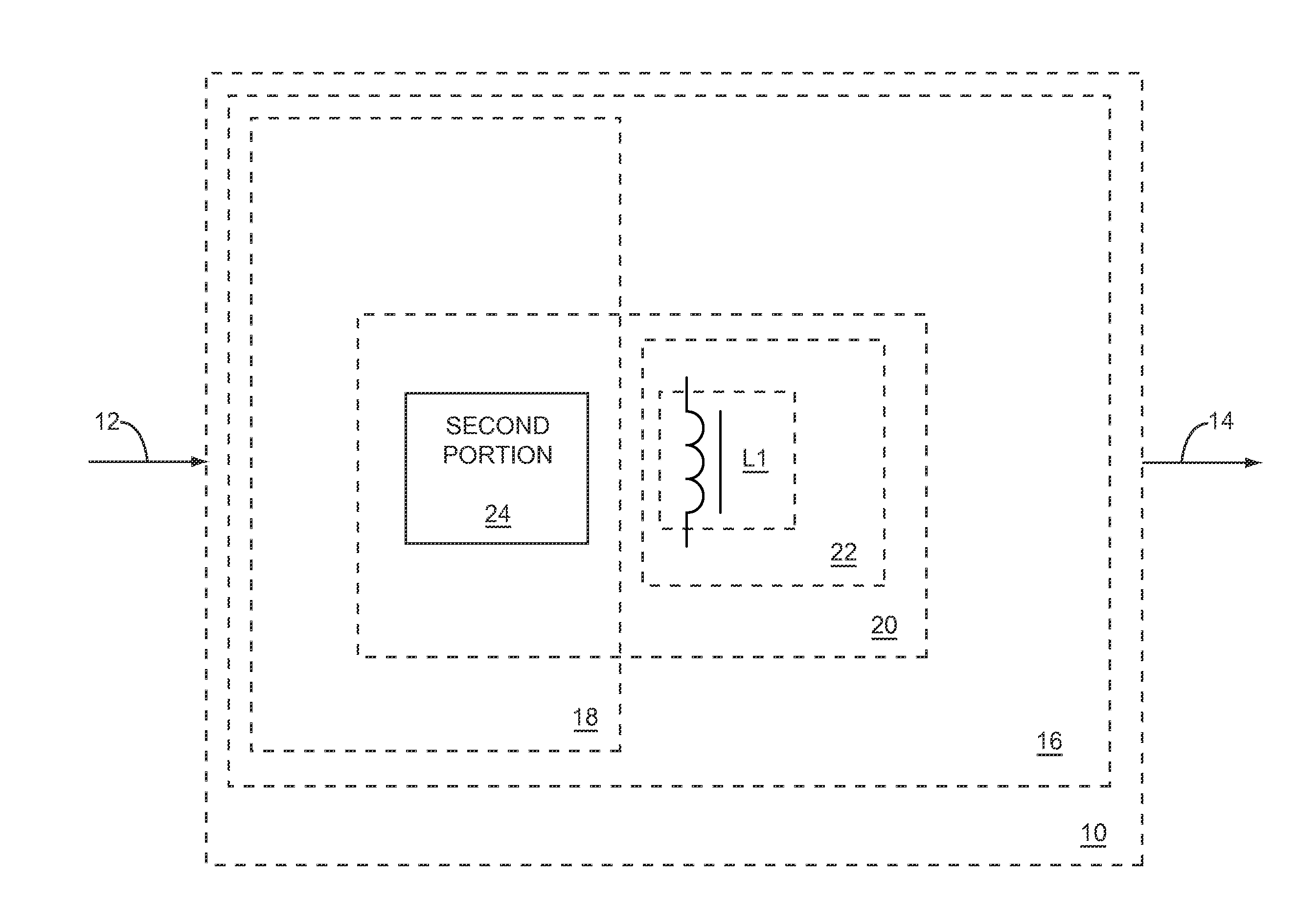
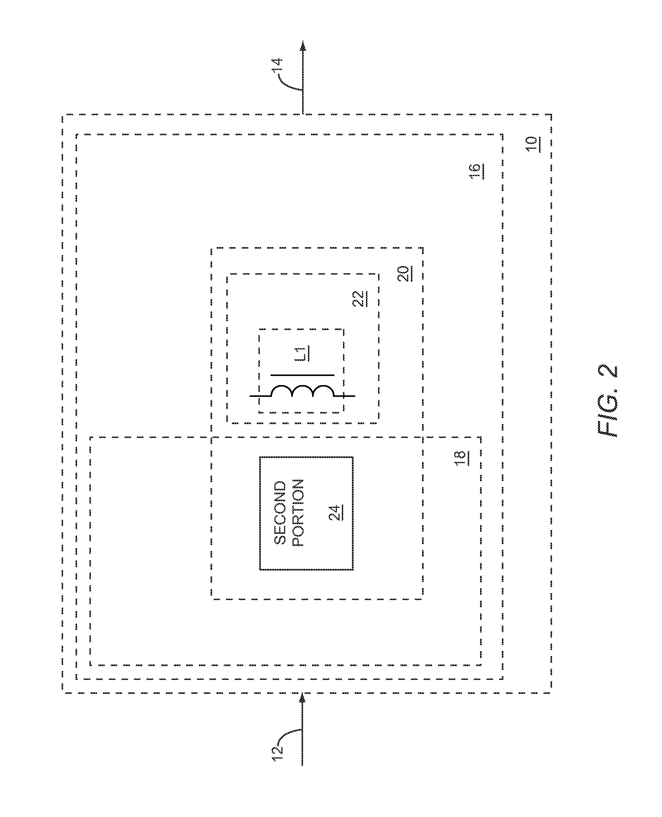
[0005]The present disclosure relates to a multi-band RF power amplifier (PA) module, which is used to receive, filter, and amplify a first RF input signal to provide a first RF output signal using a first tunable bandpass and notch filter. The multi-band RF PA module may include a supporting substrate having at least a first inductive element that provides a first portion of the first tunable bandpass and notch filter. Further, the multi-band RF PA module may include at least a first semiconductor die, which is attached to the supporting substrate and provides a second portion of the first tunable bandpass and notch filter. A transceiver module may provide the first RF input signal, which may be a first RF transmit signal, to the multi-band RF PA module, such that the first tunable bandpass and notch filter may reduce a noise spur from the transceiver module or may reduce RF receive band noise from the transceiver module, which may relax transceiver module receive noise floor requir...
PUM
 Abstract
Description
Claims
Application Information