Implementing chip to chip calibration within a TSV stack

a technology of tsv stack and chip, applied in the field of data processing, can solve the problems of consuming margin, affecting the setup or hold timing margin, and limiting the performance of the subsystem comprised of the chips by the lowest performing parts of the group

Active Publication Date: 2014-04-08
INT BUSINESS MASCH CORP
View PDF11 Cites 16 Cited by
  • Summary
  • Abstract
  • Description
  • Claims
  • Application Information

AI Technical Summary

Benefits of technology

[0014]Principal aspects of the present invention are to provide a method and circuit for implementing a chip to chip calibration with through silicon vias (TSV) stack, and a design structure on which the subject circuit resides. Other important aspects of the present invention are to provide such method, circuit, and design structure substantially without negative effects and that overcome many of the disadvantages of prior art arrangements.
[0015]In brief, a method and circuit for implementing a chip to chip calibration in a chip stack, for example, with through silicon vias (TSV) stack, and a design structure on which the subject circuit resides are provided. A first chip and a second chip are included within a semiconductor chip stack. The semiconductor chip stack includes a vertical stack optionally provided with Though Silicon Via (TSV) stacking of the chips. At least one of the first chip and the second chip includes a calibration control circuit and a performance indicator circuit coupled to the calibration control circuit to train and calibrate at least one of the first chip and the second chip to provide enhanced performance and reliability for the semiconductor chip stack.
[0018]In accordance with features of the invention, the calibration logic samples the performance indicators of the chips of the TSV stack and compares them. Depending on the parameters to be matched, the calibration logic selectively raises or lowers the voltage control of either or both chips independently. Multiple factors affect the performance of the chips being adjusted, including for example voltage levels, process variation, temperature, intrinsic technology capability, jitter, noise, and position in the stack can add factors, such as temperature. Each such multiple factors affect the performance of the chips being adjusted to varying degree. For example, higher voltage increases the performance of the chip and allows the chip to better match the performance of the other chip. This is done when a chip is lower in performance than the other chips in the system or lower than the performance required to operate in the system. A lower voltage decreases the performance of the chip but also saves power. This is desirable if one chip is faster than required to operate in the system and can therefore sacrifice performance in order to lower power consumption.

Problems solved by technology

When two or more chips must operate using a synchronous interface, the performance of the subsystem comprised of the chips is limited by the lowest performing parts of the group.
If the strobe is misplaced to either side of the center of the eye, either setup or hold timing margins will be affected.
This misplacement can be such that the margin is consumed and the data can no longer effectively captured, as is shown in FIG. 2.
In this case, the more skew between the data bits closes the effective data eye for the strobe and, therefore, reduces the available margin for the bus and increases the challenge of where to best place the strobe.

Method used


Image

  • Implementing chip to chip calibration within a TSV stack
  • Implementing chip to chip calibration within a TSV stack
  • Implementing chip to chip calibration within a TSV stack

Examples


Embodiment Construction

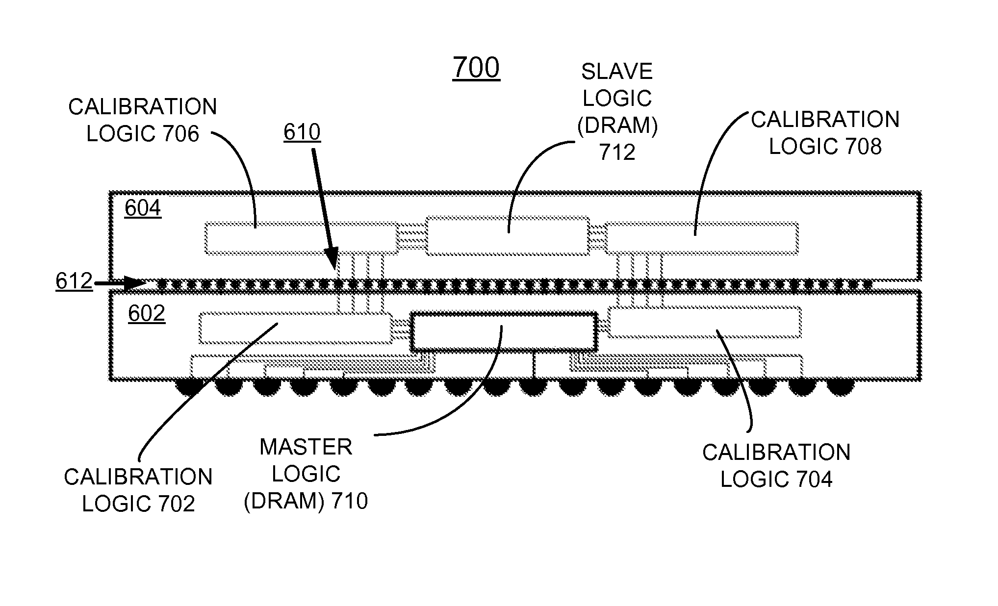
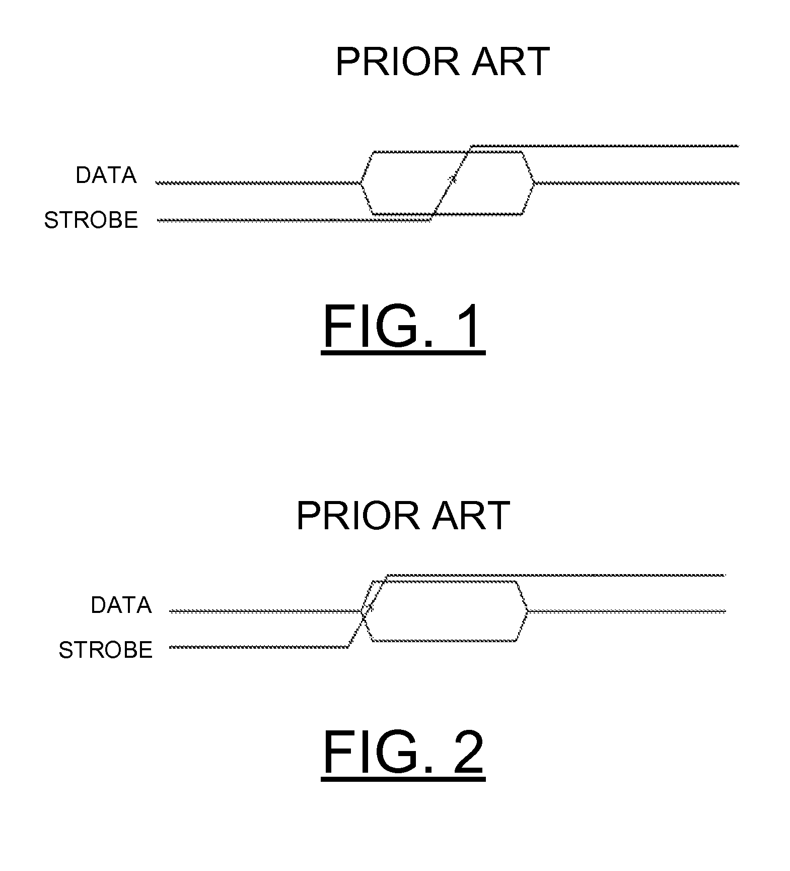
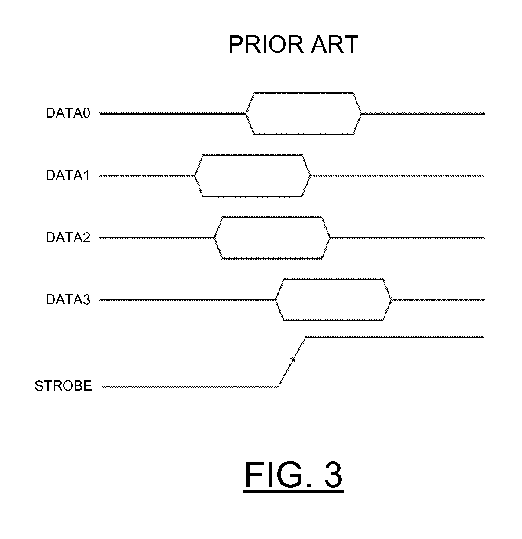
[0034]In the following detailed description of embodiments of the invention, reference is made to the accompanying drawings, which illustrate example embodiments by which the invention may be practiced. It is to be understood that other embodiments may be utilized and structural changes may be made without departing from the scope of the invention.

[0035]The terminology used herein is for the purpose of describing particular embodiments only and is not intended to be limiting of the invention. As used herein, the singular forms “a”, “an” and “the” are intended to include the plural forms as well, unless the context clearly indicates otherwise. It will be further understood that the terms “comprises” and / or “comprising,” when used in this specification, specify the presence of stated features, integers, steps, operations, elements, and / or components, but do not preclude the presence or addition of one or more other features, integers, steps, operations, elements, components, and / or gr...


PUM


Abstract

A method and circuit for implementing a chip to chip calibration in a chip stack, for example, with through silicon vias (TSV) stack, and a design structure on which the subject circuit resides are provided. A first chip and a second chip are included within a semiconductor chip stack. The semiconductor chip stack includes a vertical stack optionally provided with Though Silicon Via (TSV) stacking of the chips. At least one of the first chip and the second chip includes a calibration control circuit and a performance indicator circuit coupled to the calibration control circuit to train and calibrate at least one of the first chip and the second chip to provide enhanced performance and reliability for the semiconductor chip stack.

Description

FIELD OF THE INVENTION[0001]The present invention relates generally to the data processing field, and more particularly, relates to a method and circuit for implementing a chip to chip calibration with through silicon vias (TSV) stack, and a design structure on which the subject circuit resides.DESCRIPTION OF THE RELATED ART[0002]In a system which connects two or more electrical components, such as semiconductor chips, the timing of the signals between the components may be critical. The timing properties which are important may be such things as clock period, clock duty cycle and signal to signal relative arrival times. These relationships and properties are particularly important in synchronous interfaces, such as clocked and / or strobed busses.[0003]When two or more chips must operate using a synchronous interface, the performance of the subsystem comprised of the chips is limited by the lowest performing parts of the group. Performance of a semiconductor chip can be altered by mo...

Claims


Application Information

Patent Timeline
Patent Type & Authority Patents(United States)
IPC IPC(8): G01R35/00
CPCH01L25/18H01L2225/06513H01L2224/16H01L25/0657H01L2225/06541G06F1/10
Inventor CORDERO, EDGAR R.KUMAR, DIVYASAETOW, ANUWATTREMAINE, ROBERT B.
Owner INT BUSINESS MASCH CORP
Why Eureka
Try Eureka