Semiconductor package with integrated metal pillars and manufacturing methods thereof

a technology of metal pillars and semiconductors, applied in semiconductor devices, semiconductor/solid-state device details, electrical apparatus, etc., can solve the problems of limiting the extent to which a package having the conventional structure can be miniaturized, cracking at lower values of tensile stress, etc., and achieve the effect of reducing a maximum stress

Active Publication Date: 2014-04-15
ADVANCED SEMICON ENG INC
View PDF114 Cites 14 Cited by
  • Summary
  • Abstract
  • Description
  • Claims
  • Application Information

AI Technical Summary

Benefits of technology

[0012]In another embodiment, the semiconductor package includes a substrate and a semiconductor device. The semiconductor device comprises: (1) a body; (2) a dielectric layer disposed adjacent to the body, wherein the dielectric layer is subject to stress resulting from a mismatch of coefficient of thermal expansion (CTE) between the substrate and the semiconductor device; and (3) means for reducing a maximum stress on the dielectric layer to protect the dielectric layer from at least one of cracking and delamination.

Problems solved by technology

This can limit the extent to which a package having the conventional structure can be miniaturized.
The ultra low k and extremely low k dielectric layers tend to have low tensile strength, which can result in cracking at lower values of tensile stress than for higher k dielectric layers.

Method used


Image

  • Semiconductor package with integrated metal pillars and manufacturing methods thereof
  • Semiconductor package with integrated metal pillars and manufacturing methods thereof
  • Semiconductor package with integrated metal pillars and manufacturing methods thereof

Examples


Embodiment Construction

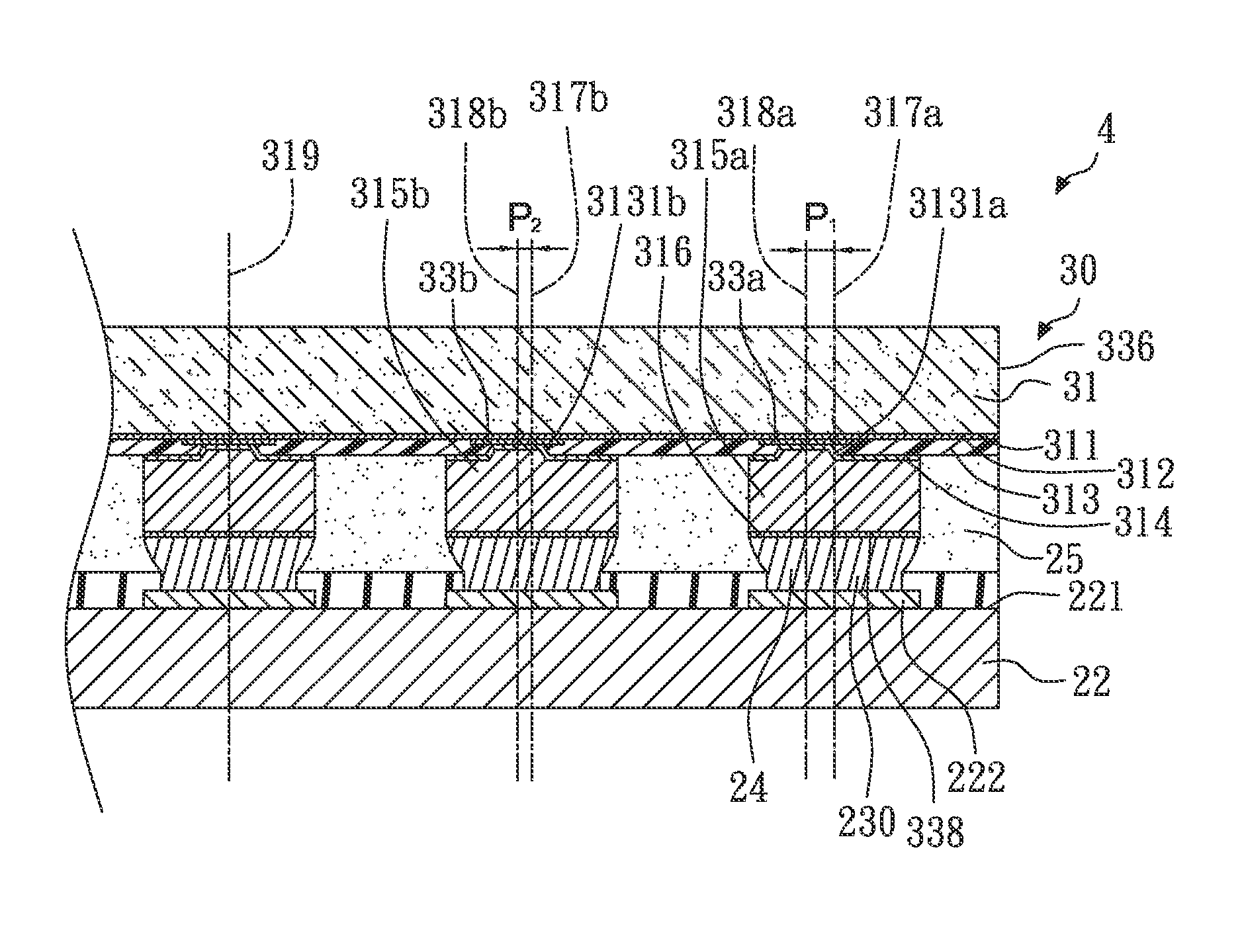
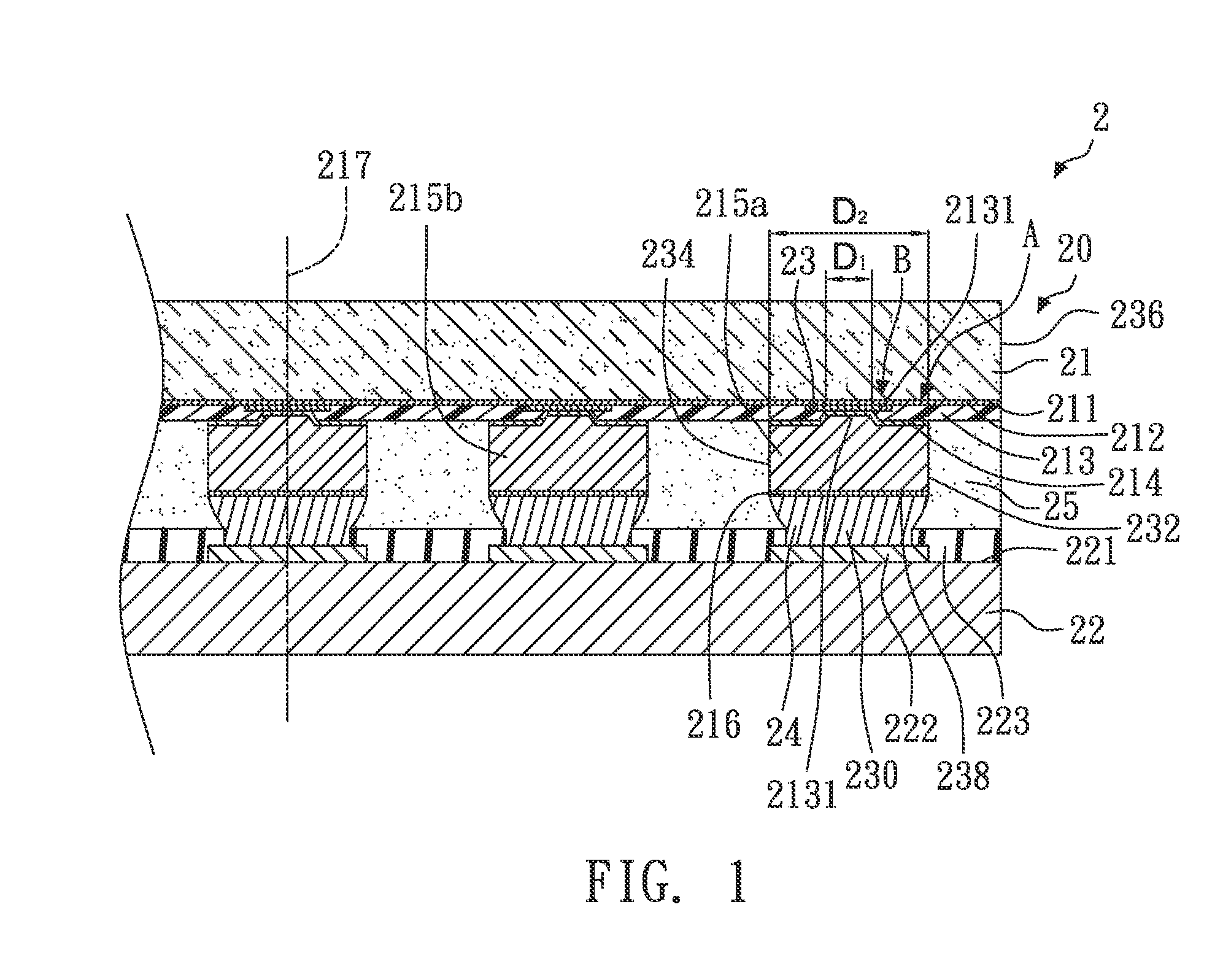
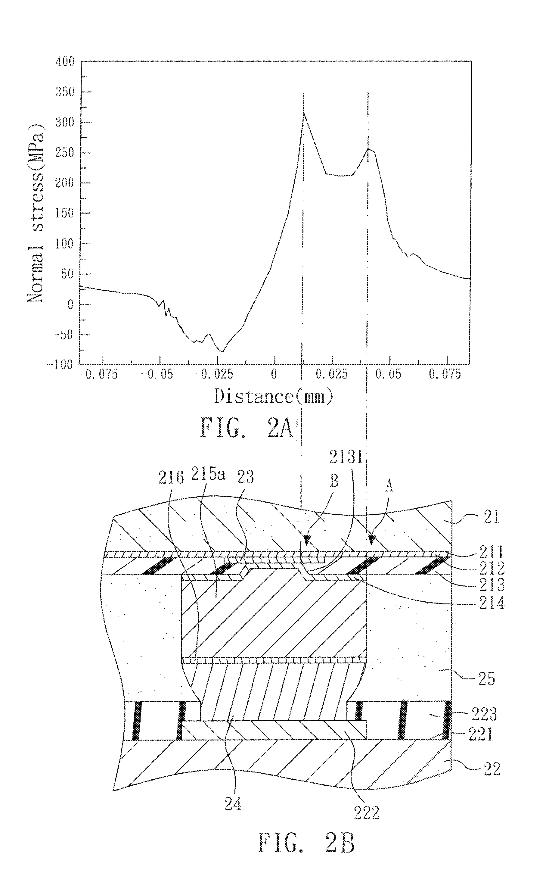
[0022]Referring to FIG. 1, a cross section view of a semiconductor package 2 according to an embodiment of the invention is illustrated. The package 2 includes a substrate 22, at least one electrical connector 24 (for example, conductive solder), a semiconductor device 20, and an underfill layer 25. In the illustrated embodiment, the semiconductor device 20 is a semiconductor chip, although it is contemplated that the semiconductor device 20, in general, can be any active device such as an active electronic component, any passive device, or a combination thereof. The semiconductor device 20 may be disposed adjacent to the electrical connector 24. The semiconductor device 20 may be bonded to the electrical connector 24 by flip chip bonding. The substrate 22 includes an upper surface 221, at least one substrate pad 222, and a solder mask layer 223. The substrate 22 may be an organic substrate. In one embodiment, the solder mask layer 223 is disposed adjacent to the upper surface 221, ...


PUM


Abstract

A semiconductor package includes a substrate and a semiconductor device. The semiconductor device includes a body having a center, a layer disposed adjacent to the body, and a plurality of conductive pillars configured to electrically connect the semiconductor device to the substrate. The layer defines a plurality of openings. Each of the plurality of conductive pillars extends at least partially through a corresponding one of the plurality of openings. An offset between a first central axis of the each of the plurality of conductive pillars and a second central axis of the corresponding one of the plurality of openings varies with distance between the first central axis and the center of the body. The second central axis of the corresponding one of the plurality of openings is disposed between the first central axis of the each of the plurality of conductive pillars and the center of the body.

Description

CROSS-REFERENCE TO RELATED APPLICATION[0001]This application claims the benefit of Taiwan Patent Application No. 099132517, filed on Sep. 27, 2010, the subject matter of which is incorporated herein by reference.BACKGROUND OF THE INVENTION[0002]1. Field of the Invention[0003]The present invention relates generally to semiconductor packages and manufacturing methods thereof. More particularly, the invention relates to semiconductor packages with integrated metal pillars and manufacturing methods thereof.[0004]2. Description of Related Art[0005]A conventional flip chip package typically includes a substrate, conductive solder, a chip, and an underfill material. The substrate can be an organic substrate having an upper surface, at least one substrate pad, and a solder mask layer. The solder mask layer can have an opening so as to expose part of the substrate pad. The chip typically includes a chip body, a chip pad, a passivation layer, and at least one under ball metal layer. The condu...

Claims


Application Information

Patent Timeline
Patent Type & Authority Patents(United States)
IPC IPC(8): H01L23/48
CPCH01L2224/16105H01L2224/13171H01L2924/01074H01L23/3171H01L2224/13099H01L2224/8114H01L2224/13076H01L2224/13139H01L2924/01075H01L24/14H01L23/49894H01L2224/05155H01L2224/05166H01L2224/05644H01L2224/16237H01L2224/73204H01L24/17H01L2924/01005H01L2924/01033H01L2224/16225H01L2224/05572H01L2924/01047H01L2924/01019H01L2924/01079H01L2224/13083H01L24/16H01L2924/10253H01L2924/014H01L2224/13155H01L2224/05647H01L2924/01023H01L21/563H01L2224/16227H01L2224/13147H01L2224/14104H01L2224/13027H01L2924/01029H01L2224/13144H01L2224/05171H01L2924/01024H01L2924/00014H01L2224/0401H01L2224/1308H01L2924/00H01L2224/05552H01L2924/00012
Inventor SHIH, MENG-KAILEE, CHANG-CHI
Owner ADVANCED SEMICON ENG INC
Why Eureka
Try Eureka