Semiconductor device and method for manufacturing the same

a semiconductor and semiconductor technology, applied in the direction of semiconductor devices, semiconductor/solid-state device details, electrical equipment, etc., can solve the problems of poor reliability after mounting, the warpage of the substrate, so as to reduce the stress on the joining portions between the chip and the substrate, reduce the effect of warpag

Active Publication Date: 2014-04-29
RENESAS ELECTRONICS CORP
View PDF13 Cites 14 Cited by
  • Summary
  • Abstract
  • Description
  • Claims
  • Application Information

AI Technical Summary

Benefits of technology

[0017]As described above, it is difficult to restrain warpage of a substrate to increase the flatness of the substrate, and reduce the stress to be applied to the joining portions between a chip and the substrate due to the difference in thermal expansion coefficient between the first resin and the second resin.
[0019]In this semiconductor device, in the case of the thermal expansion coefficient of the substrate is higher than the thermal expansion coefficient of the first resin, a resin that has a higher thermal expansion coefficient than the thermal expansion coefficient of the first resin located inside is used as the second resin located outside. With this arrangement, the effect of the second resin to correct the warpage of the substrate can be made greater. Accordingly, the flatness of the substrate can be made higher. As a result, the yield and reliability of the semiconductor device in terms of mounting can be improved.
[0020]Since the first resin is formed in the formation region of the bumps located on the outermost circumference of all the bumps and is also formed inside the formation region, the joining portions between the chips including the bumps and the substrate are covered with the same resin, which is the first resin. With this arrangement, the stress to be applied to the joining portions due to the difference in thermal expansion coefficient between the resins can be restrained, though such stress cannot be restrained where two kinds of resins having different thermal expansion coefficients from each other are in contact with the same bump joining portion at both sides.
[0022]According to the present invention, warpage of the substrate can be restrained, and the flatness of the substrate can be made higher. Also, the stress to be applied to the joining portions between the chip and the substrate due to the difference in thermal expansion coefficient between the first resin and the second resin can be reduced.

Problems solved by technology

As a result, the package mounting properties and the reliability after the mounting become poorer.
As described above, it is difficult to restrain warpage of a substrate to increase the flatness of the substrate, and reduce the stress to be applied to the joining portions between a chip and the substrate due to the difference in thermal expansion coefficient between the first resin and the second resin.

Method used


Image

  • Semiconductor device and method for manufacturing the same
  • Semiconductor device and method for manufacturing the same
  • Semiconductor device and method for manufacturing the same

Examples


first embodiment

[First Embodiment]

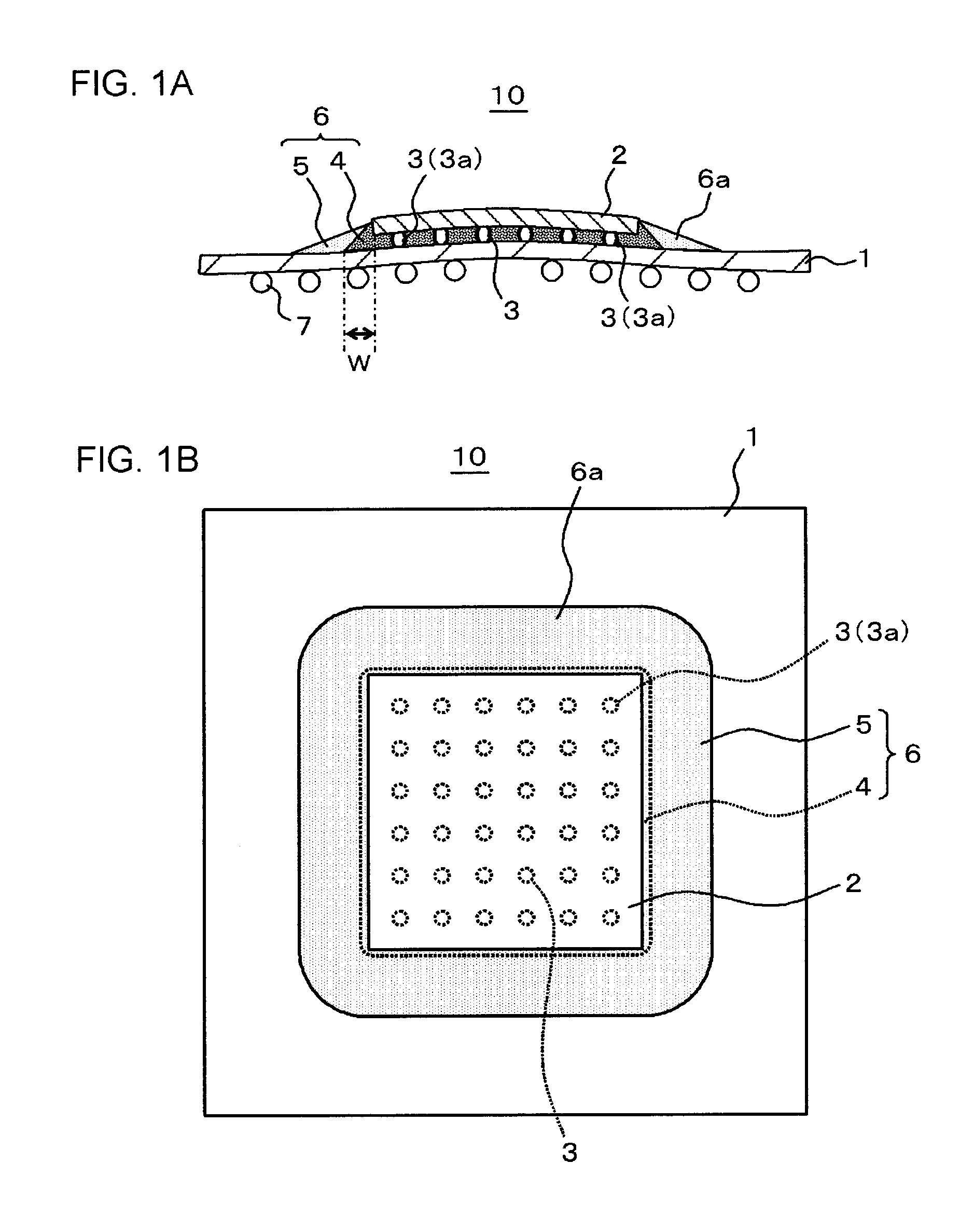
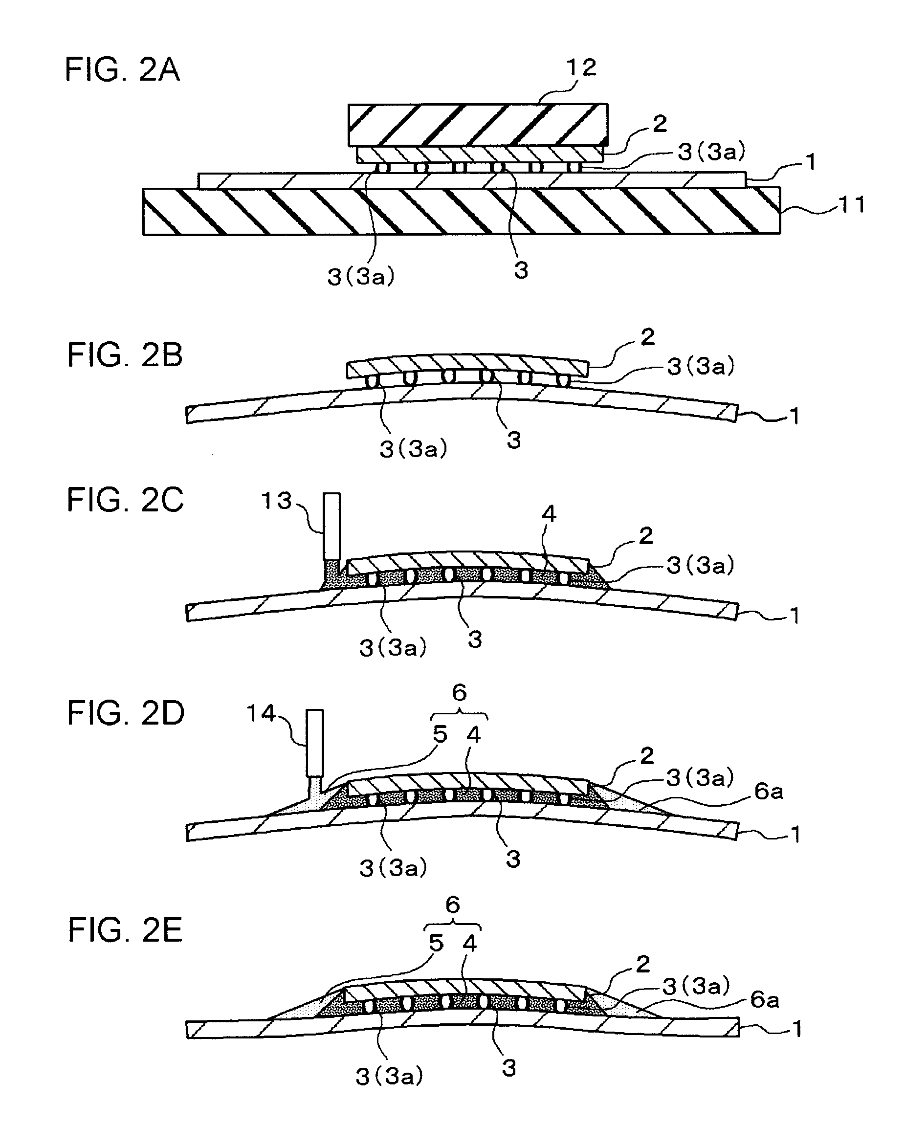
[0052]FIGS. 1A and 1B are schematic views showing the structure of a semiconductor device 10 according to a first embodiment. FIG. 1A is a front cross-sectional view, and FIG. 1B is a plan view. FIGS. 2A through 2E are a series of process drawings (cross-sectional views) for explaining a method for manufacturing the semiconductor device according to the first embodiment.

[0053]The semiconductor device 10 according to this embodiment includes a substrate 1, a semiconductor chip 2 that is connected to one of the faces of the substrate 1 via bumps 3, and has a device formation face facing the one of the faces of the substrate 1, and a resin 6 that fills the space between the device formation face of the semiconductor chip 2 and the one of the faces of the substrate 1. The resin 6 includes a first resin 4 that is formed in the formation region of bumps 3a located on the outermost circumference of the bumps 3 and is also formed inside the formation region, and a second r...

second embodiment

[Second Embodiment]

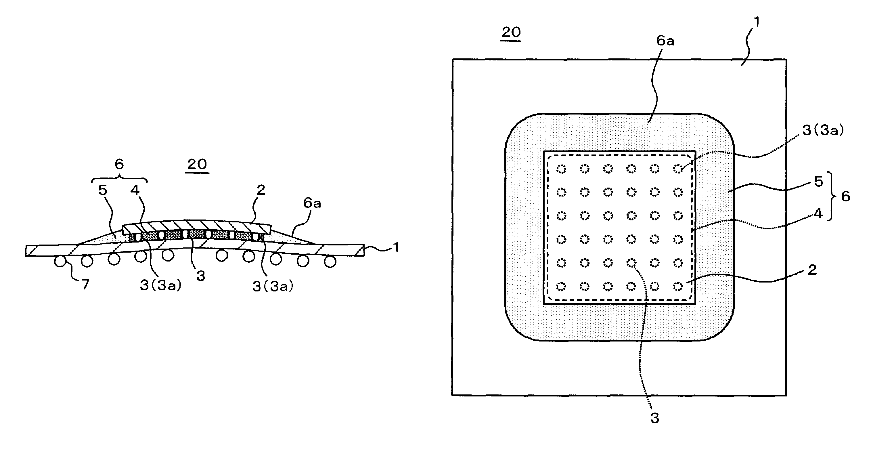
[0097]FIGS. 3A and 3B are schematic views showing the structure of a semiconductor device 20 according to a second embodiment. FIG. 3A is a front cross-sectional view, and FIG. 3B is a plan view. FIGS. 4A through 4E are a series of process drawings (cross-sectional views) for explaining a method for manufacturing the semiconductor device according to the second embodiment.

[0098]A method for manufacturing the semiconductor device 20 according to this embodiment differs from the manufacturing method according to the first embodiment. In this embodiment, the first resin 4 is supplied (or placed) onto the substrate 1 prior to the flip-chip bonding, and after the flip-chip bonding, the second resin 5 is supplied. Accordingly, not only a liquid resin that is supposedly used in the first embodiment, but also a film-type resin may be used as the first resin 4.

[0099]Referring now to FIGS. 4A through 4E, the method for manufacturing the semiconductor device according to thi...

third embodiment

[Third Embodiment]

[0113]FIGS. 5A and 5B are schematic views showing a semiconductor device 30 according to a third embodiment. FIG. 5A is a front cross-sectional view, and FIG. 5B is a plan view.

[0114]As shown in FIGS. 5A and 5B, this embodiment differs from the first embodiment in the arrangement of the bumps 3. In the first and second embodiments, the bumps 3 are arranged in the so-called “area-arrangement” manner in the plane of the chip 2. In this embodiment, on the other hand, the bumps 3 are arranged along the peripheral portion of the chip 2 (arranged in a so-called “peripheral-arrangement” manner).

[0115]The other aspects of the semiconductor device 30 according to this embodiment are the same as those of the first or second embodiment, and the semiconductor device 30 achieves the same effects as those of the first or second embodiment.


PUM


Abstract

A semiconductor device includes a substrate, a semiconductor chip that is bonded to one of the faces of the substrate via bumps, and has a device formation face facing the one of the faces, and a resin that fills the space between the device formation face of the semiconductor chip and the one of the faces of the substrate. The resin includes: a first resin that is formed in a formation region of bumps placed on the outermost circumference of the bumps, and is formed inside the formation region, and a second resin that is formed outside the first resin. The thermal expansion coefficient of the substrate is higher than the thermal expansion coefficient of the first resin. The thermal expansion coefficient of the second resin is higher than the thermal expansion coefficient of the first resin.

Description

[0001]This application is based on Japanese patent application No. 2009-237128, the content of which is incorporated hereinto by reference.BACKGROUND[0002]1. Technical Field[0003]The present invention relates to a semiconductor device and a method for manufacturing the semiconductor device.[0004]2. Related Art[0005]In recent years, there has been an increasing demand for semiconductor devices (semiconductor packages (hereinafter referred to as packages)) each having a semiconductor chip (hereinafter referred to as a chip) and a semiconductor substrate (hereinafter referred to as a substrate) electrically connected to each other by a flip-chip process. Such semiconductor packages are demanded as small-area, thin packages that can be mounted at a high density.[0006]The flip-chip process can be performed in the following manner. First, the surface (the circuit formation face) of a chip and the interconnect face (the side on which the interconnects for the chip are formed) of a substrat...

Claims


Application Information

Patent Timeline
Patent Type & Authority Patents(United States)
IPC IPC(8): H01L29/66
CPCH01L2224/92125H01L2224/75743H01L2224/75H01L24/27H01L2924/18161H01L2924/3511H01L2224/48227H01L21/563H01L2224/49173H01L24/81H01L2224/81801H01L2224/83102H01L2924/15311H01L2224/81203H01L2224/83104H01L2224/48091H01L2224/73204H01L25/50H01L23/3135H01L2924/01079H01L24/16H01L24/13H01L2224/73203H01L2924/01322H01L2224/32225H01L2224/83192H01L2225/06517H01L2224/49171H01L2224/83951H01L2924/01078H01L2224/75251H01L24/48H01L2224/73265H01L2225/0651H01L24/49H01L24/83H01L2924/01029H01L2224/16225H01L24/75H01L2224/75252H01L2224/81191H01L2224/32145H01L25/0657H01L2224/451H01L2224/45144H01L2224/45147H01L24/45H01L24/73H01L2924/181H01L2924/00014H01L2924/00012H01L2924/00H01L2924/3512
Inventor SAKATA, KENJIKIDA, TSUYOSHI
Owner RENESAS ELECTRONICS CORP
Why Eureka
Try Eureka