Semiconductor packaging method, semiconductor packaging structure and packaging body

A packaging method and packaging structure technology, which is applied in the direction of semiconductor devices, semiconductor/solid-state device manufacturing, semiconductor/solid-state device components, etc., can solve problems such as lower reliability, affecting the structural performance of the package, and increasing the packaging height of electronic components , to achieve the effect of reducing the height

Pending Publication Date: 2021-04-16
CHANGXIN MEMORY TECH INC
View PDF0 Cites 4 Cited by
  • Summary
  • Abstract
  • Description
  • Claims
  • Application Information

AI Technical Summary

Problems solved by technology

With the development of the electronics industry, there is an increasing need for high capacity, high functionality, high speed, and small size of electronic components. In order to meet this demand, more chips need to be incorporated into a single package, which leads to a higher package height of electronic components , the reliability becomes lower, which affects the performance of the package structure

Method used


Image

  • Semiconductor packaging method, semiconductor packaging structure and packaging body
  • Semiconductor packaging method, semiconductor packaging structure and packaging body
  • Semiconductor packaging method, semiconductor packaging structure and packaging body

Examples


Embodiment Construction

[0026] Specific implementations of the semiconductor packaging method, semiconductor packaging structure, and packaging body provided by the present invention will be described in detail below in conjunction with the accompanying drawings.

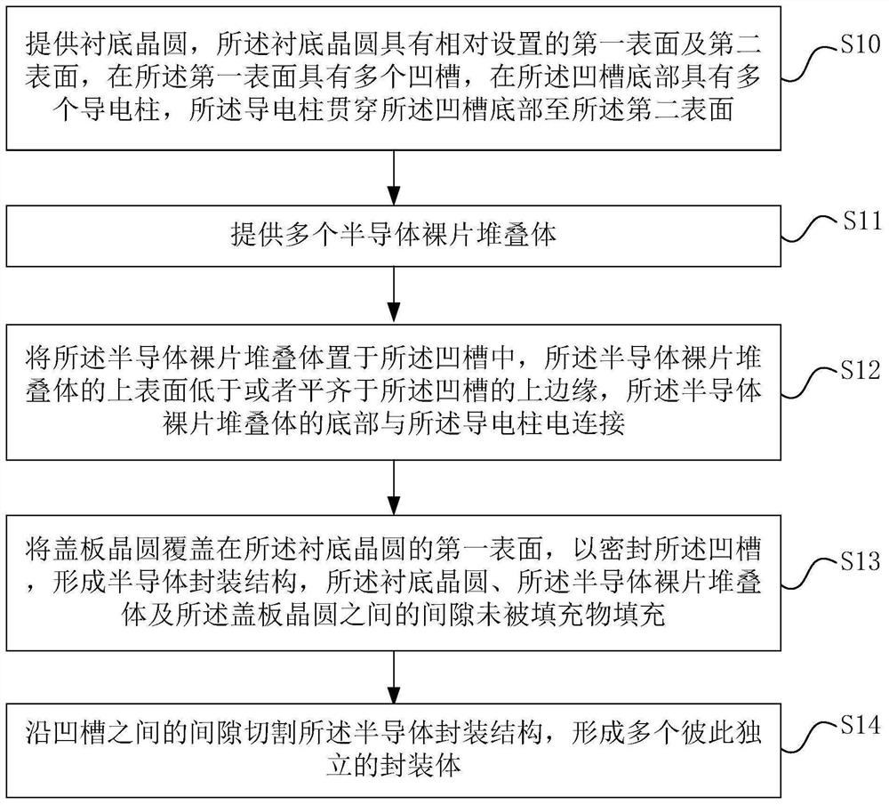
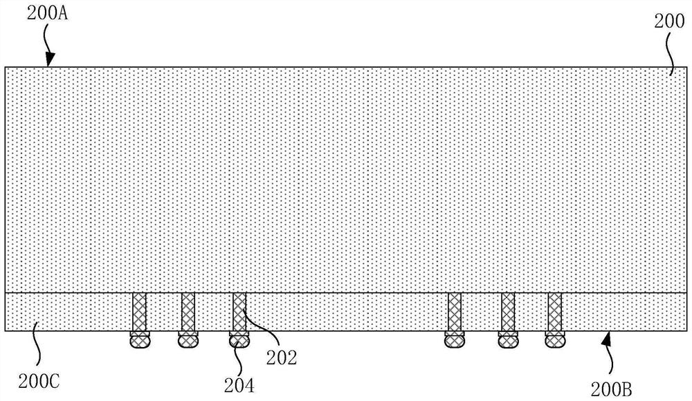
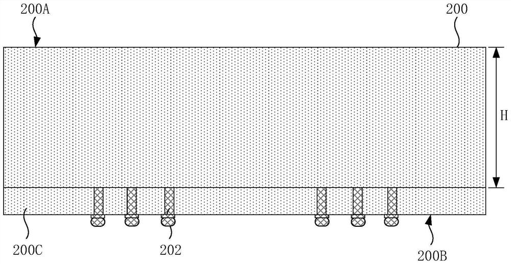
[0027] figure 1 It is a schematic diagram of the steps of a specific embodiment of the semiconductor packaging method of the present invention. see figure 1 , the semiconductor packaging method includes the following steps: step S10, providing a substrate wafer, the substrate wafer has a first surface and a second surface oppositely arranged, there are a plurality of grooves on the first surface, and The bottom of the groove has a plurality of conductive pillars, and the conductive pillars pass through the bottom of the groove to the second surface; step S11, providing a plurality of semiconductor die stacks; step S12, stacking the semiconductor die The body is placed in the groove, the upper surface of the semiconductor die stack is low...


PUM


Abstract

The invention provides a semiconductor packaging method, a semiconductor packaging structure and a packaging body. The method comprises the following steps: providing a substrate wafer provided with a first surface and a second surface, wherein the first surface and the second surface are oppositely arranged, the first surface is provided with a plurality of grooves, the bottom of each groove is provided with a plurality of conductive columns, and the conductive columns penetrate through the substrate wafer; providing a plurality of semiconductor bare chip stacks; placing the semiconductor bare chip stacks in the groove, wherein the upper surface of the semiconductor bare chip stack is lower than or flush with the upper edge of the groove, and the bottom of the semiconductor bare chip stack is electrically connected with the conductive columns; and covering the first surface of the substrate wafer with the cover plate wafer to seal the groove to form a semiconductor packaging structure, wherein it is ensured that gaps among the substrate wafer, the semiconductor bare chip stack body and the cover plate wafer are not filled with the filler. The method of the invention has the advantages that the formed semiconductor structure has the characteristics of low packaging height, high reliability and low warping degree.

Description

technical field [0001] The invention relates to the field of semiconductor packaging, in particular to a semiconductor packaging method, a semiconductor packaging structure and a packaging body. Background technique [0002] Stacked packaging technology, also known as 3D or three-dimensional packaging technology, is one of the mainstream multi-chip packaging technologies at present. Blocks with complete functions) are superimposed in the vertical direction and are often used to manufacture electronic components such as memory chips, logic chips, and processor chips. With the development of the electronics industry, there is an increasing need for high capacity, high functionality, high speed, and small size of electronic components. In order to meet this demand, more chips need to be incorporated into a single package, which leads to a higher package height of electronic components , the reliability becomes lower, which affects the performance of the package structure. [...

Claims


Application Information

Patent Timeline
Patent Type & Authority Applications(China)
IPC IPC(8): H01L21/52H01L21/60H01L21/48H01L23/538
CPCH01L23/538H01L21/48H01L21/52H01L2224/16145H01L2224/16146H01L2224/17181H01L2224/94H01L2224/95H01L2224/97H01L24/81H01L24/94H01L24/95H01L24/97H01L25/0657H01L2225/06513H01L2225/06517H01L2225/06541H01L2225/06548H01L25/105H01L25/50H01L2924/00014H01L23/055H01L23/562H01L2224/06181H01L2924/15311H01L2924/15153H01L2225/06565H01L2225/06586H01L2225/06589H01L2224/16235H01L2924/3511H01L2224/81H01L2224/13099H01L21/78H01L23/481H01L24/16H01L2224/16148H01L2224/16221
Inventor 刘杰应战
Owner CHANGXIN MEMORY TECH INC
Why Eureka
Try Eureka