Direct connect single layer touch panel

a touch sensor and direct connection technology, applied in the direction of optics, instruments, printed circuits, etc., can solve the problems of high manufacturing cost of flex circuit fabrication, high cost of bonding to both sides of the substrate, and the drive and sense lines formed on the bottom and top sides of a single substrate, so as to simplify the manufacturing process of the substrate

Inactive Publication Date: 2014-04-29
APPLE INC
View PDF40 Cites 9 Cited by
  • Summary
  • Abstract
  • Description
  • Claims
  • Application Information

AI Technical Summary

Benefits of technology

[0004]This relates to a substantially transparent touch sensor panel having co-planar single-layer touch sensors and traces fabricated on a single side of a substrate for detecting single or multi-touch events (the touching of one or multiple fingers or other objects upon a touch-sensitive surface at distinct locations at about the same time). To avoid having to fabricate conductive layers on different sides of the substrate, embodiments of the disclosure can form the touch sensor elements and their corresponding traces in a single layer on one side of the substrate.
[0006]By using the board as the dielectric to connect traces from multiple sensor elements in each row, rather than using a dielectric layer on the substrate upon which the sensor elements and traces are formed, the sensor elements and traces on the substrate can be formed by simply patterning a single layer of conductive material on the substrate. This can simplify the manufacturing process of the substrate from a complexity and cost perspective. In other words, the processes needed to allow some traces to cross over other traces without shorting to each other to provide the necessary connectivity can be avoided when the board is used, because the board can provide vias and routing on a separate layer that achieves the equivalent of electrical crossovers.

Problems solved by technology

However, touch sensor panels having drive and sense lines formed on the bottom and top sides of a single substrate can be expensive to manufacture.
Another reason can be the cost of the flex circuit fabrication and bonding to connect to both sides of the substrate.

Method used


Image

  • Direct connect single layer touch panel
  • Direct connect single layer touch panel
  • Direct connect single layer touch panel

Examples


Embodiment Construction

[0023]In the following description of preferred embodiments, reference is made to the accompanying drawings where it is shown by way of illustration specific embodiments in which the disclosure can be practiced. It is to be understood that other embodiments can be used and structural changes can be made without departing from the scope of the embodiments of this disclosure.

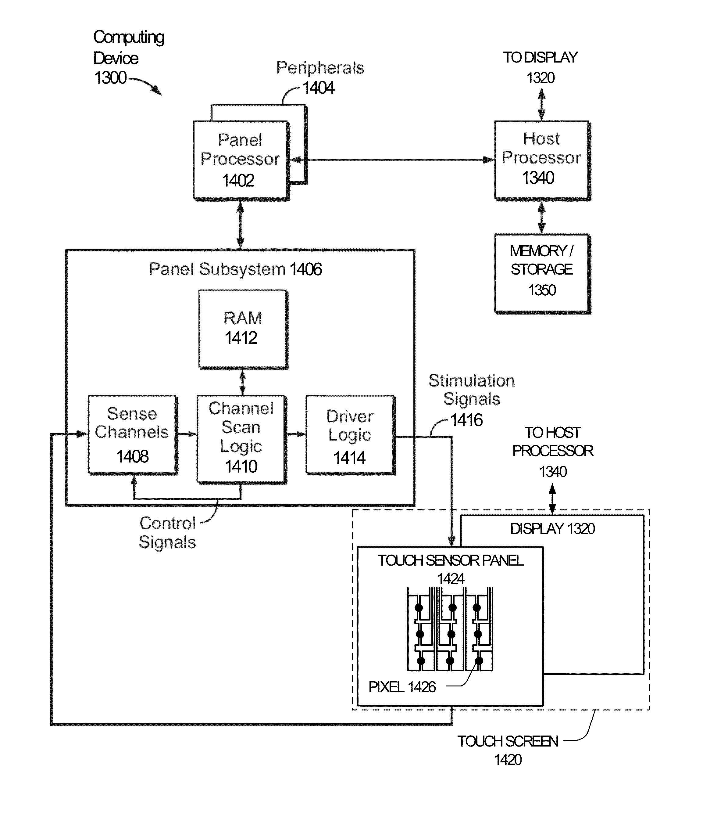
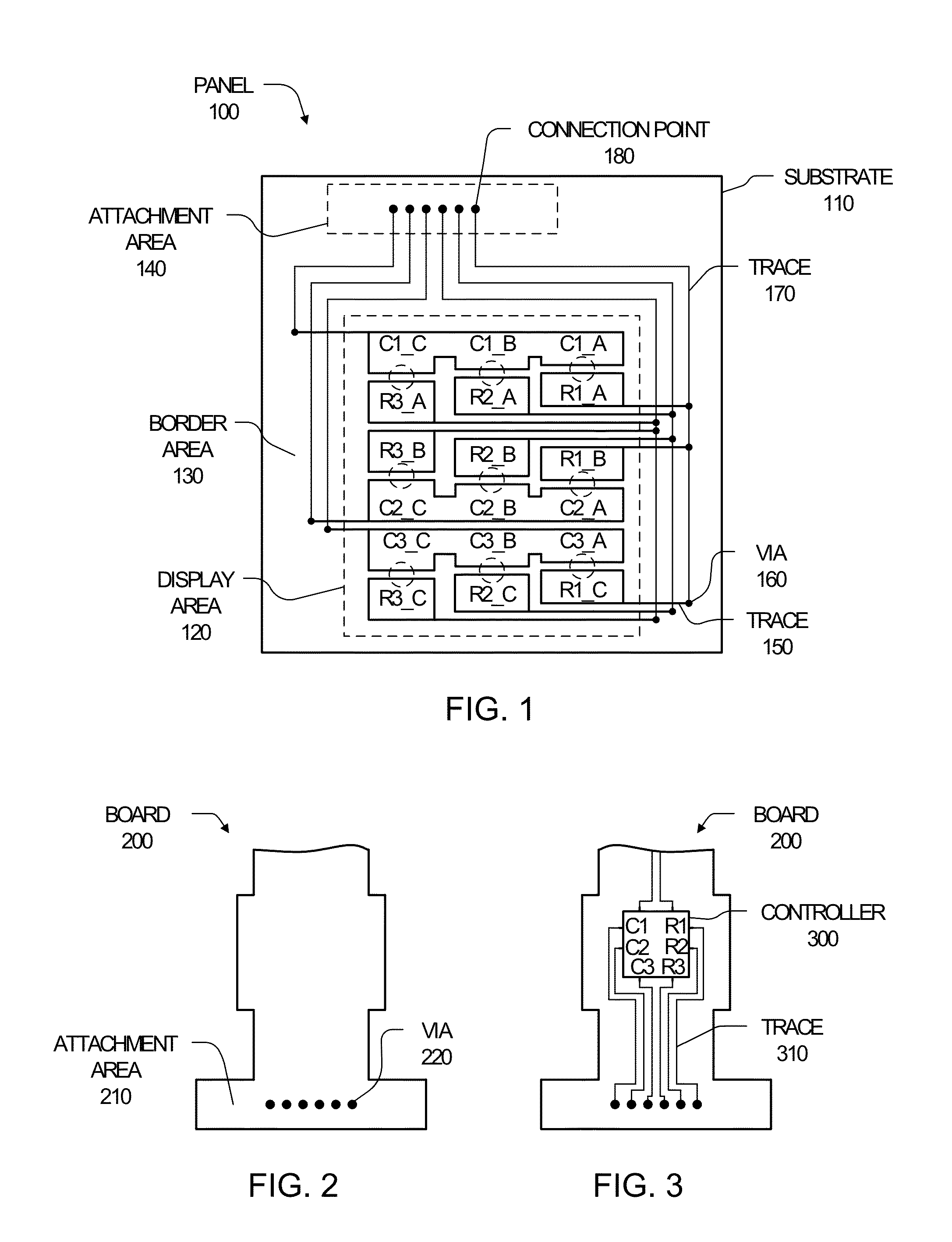
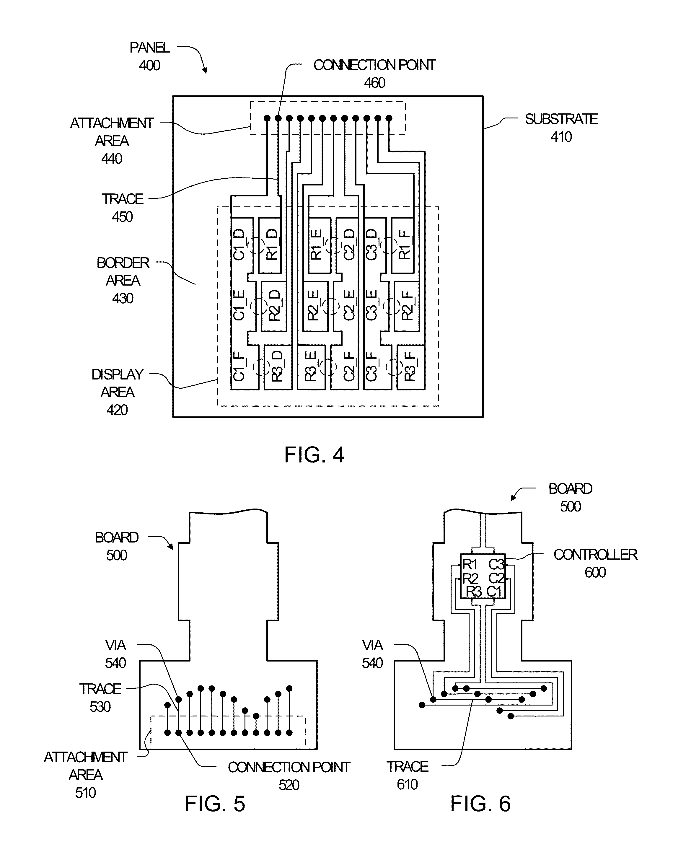
[0024]Embodiments of the disclosure relate to a substantially transparent touch sensor panel having co-planar single-layer touch sensors and traces fabricated on a single side of a substrate for detecting single or multi-touch events (the touching of one or multiple fingers or other objects upon a touch-sensitive surface at distinct locations at about the same time). To avoid having to fabricate conductive layers on different sides of the substrate, embodiments of the disclosure can form the touch sensor elements and their corresponding traces in a single layer on one side of the substrate.

[0025]The sensor element...


PUM

PropertyMeasurementUnit
electricalaaaaaaaaaa
electrical connectivityaaaaaaaaaa
conductiveaaaaaaaaaa

Abstract

A substantially transparent touch sensor panel having co-planar single-layer touch sensors and traces fabricated on a single side of a substrate for detecting single or multi-touch events. The touch sensor elements can be fabricated in columns and rows, with each sensor element in a row adjacent to a sensor element in a column. By using a board as the dielectric to connect traces from multiple sensor elements in each row, rather than using a dielectric layer on the substrate upon which the sensor elements and traces are formed, the sensor elements and traces on the substrate can be formed by simply patterning a single layer of conductive material on the substrate, which can simplify the manufacturing process of the substrate from a complexity and cost perspective.

Description

FIELD OF THE DISCLOSURE[0001]This relates generally to input devices for computing systems, and more particularly, to a multi-touch sensor panel capable of being fabricated in a single layer on one side of a substrate.BACKGROUND OF THE DISCLOSURE[0002]Many types of input devices are presently available for performing operations in a computing system, such as buttons or keys, mice, trackballs, joysticks, touch sensor panels, touch screens and the like. Touch screens, in particular, are becoming increasingly popular because of their ease and versatility of operation as well as their declining price. Touch screens can include a touch sensor panel, which can be a clear panel with a touch sensitive surface, and a display device such as a liquid crystal display (LCD) that can be positioned partially or fully behind the panel so that the touch sensitive surface can cover at least a portion of the viewable area of the display device. Touch screens can allow a user to perform various functio...

Claims


Application Information

Patent Timeline
Patent Type & Authority Patents(United States)
IPC IPC(8): G06F3/041G02F1/1345G06F3/045H05K1/00
CPCG06F3/044G06F3/0443G06F3/0446
Inventor GRUNTHANER, MARTIN PAULHOTELLING, STEVEN PORTER
Owner APPLE INC
Why Eureka
Try Eureka