Atomic force microscopy system and method for nanoscale measurement

a microscopy and nano-scale technology, applied in the field ofatomic force microscopy, can solve the problems of limited imaging of materials, damage to samples, and poor resolution and sensitivity of mfm

Active Publication Date: 2014-05-13
THE UNITED STATES OF AMERICA AS REPRESETNED BY THE SEC OF THE AIR FORCE
View PDF43 Cites 2 Cited by
  • Summary
  • Abstract
  • Description
  • Claims
  • Application Information

AI Technical Summary

Problems solved by technology

In addition, the voltage between the tip and the sample may become too high, causing damage to the sample.
Soft sample materials such as powders or biological materials are particularly prone to damage and alteration, which limits imaging of these materials.
However, the resolution and sensitivity of MFM is generally poor as compared to other methods of AFM because the required stiffness of the cantilever and imaging in non-contact mode prevents the system from being as responsive to minor changes.
This reduced responsiveness results in lower sensitivity and a poor quality, low resolution image.
Increasing the magnetic field surrounding the tip increases the resolution but it may also affect the magnetization of the sample.

Method used


Image

  • Atomic force microscopy system and method for nanoscale measurement
  • Atomic force microscopy system and method for nanoscale measurement
  • Atomic force microscopy system and method for nanoscale measurement

Examples


Embodiment Construction

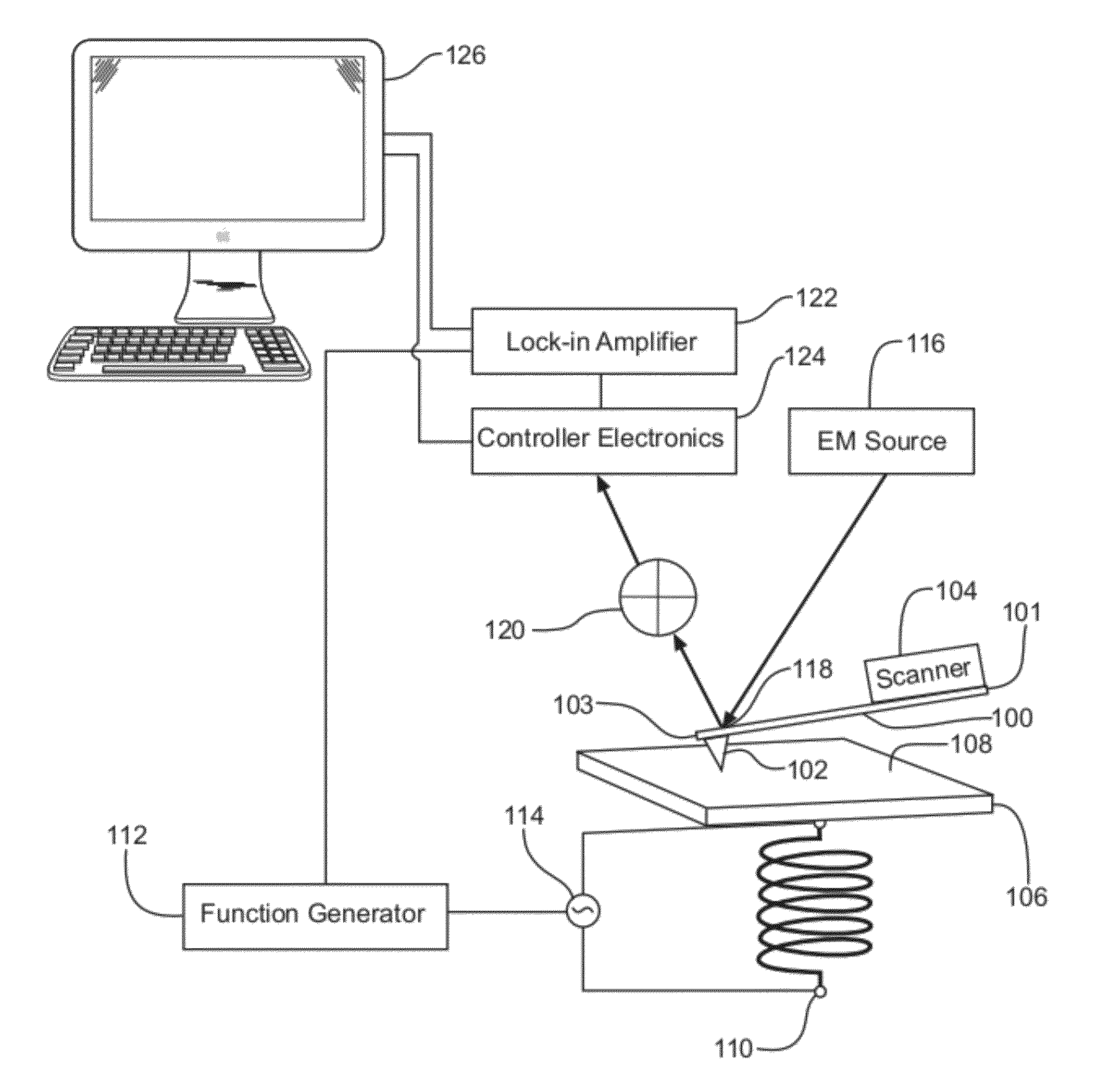
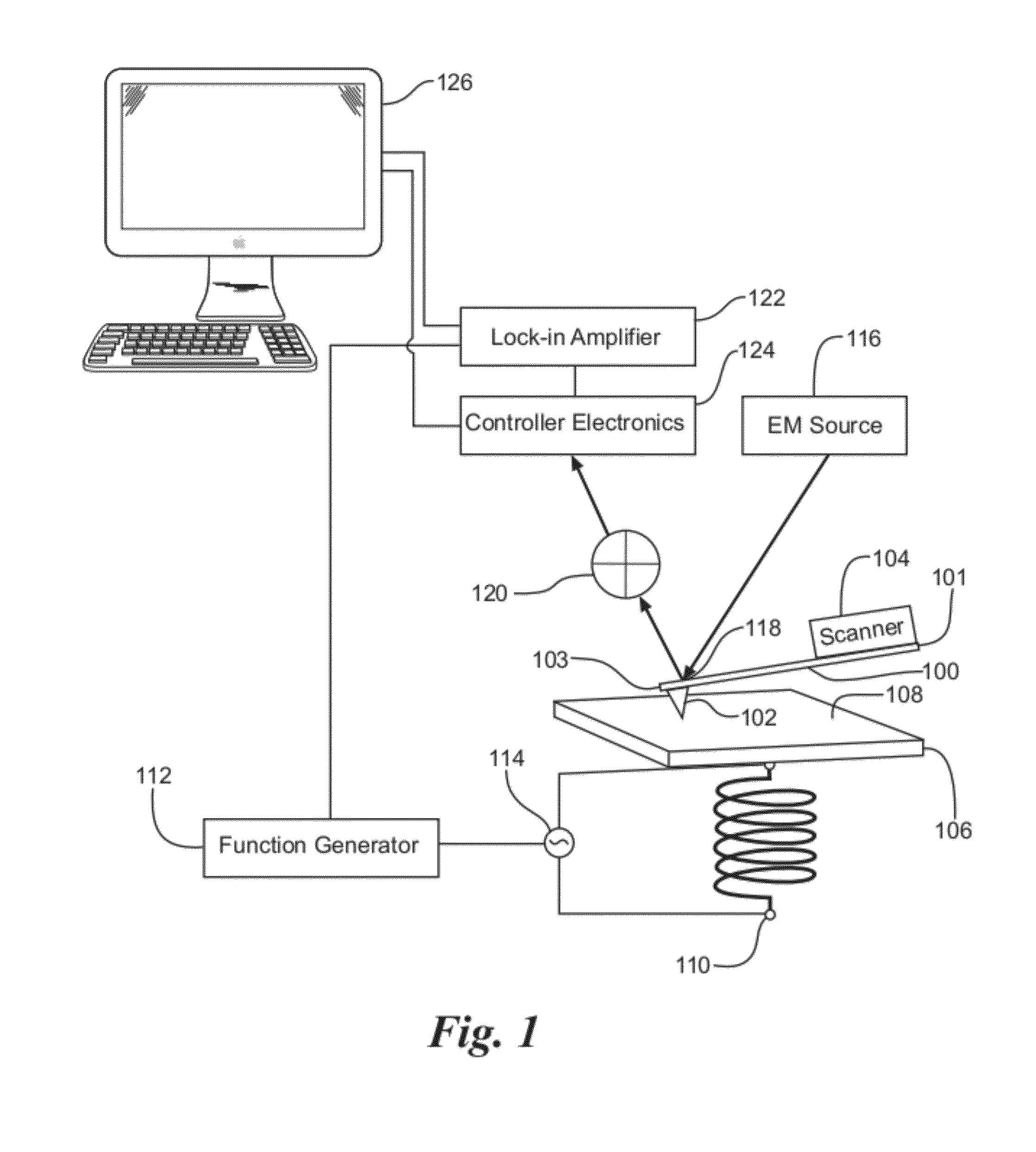
[0027]The present invention provides an atomic force microscopy (AFM) system capable of imaging multiple physical properties of a sample material at the nanoscale level with a minimum amount of alteration to the system, thereby saving valuable time and equipment costs. The present invention provides an apparatus and method for imaging physical properties using an electromagnetic coil placed under the sample. Excitation of the coil creates currents in the sample, which may then be used to image multiple properties including elastic, electrical, dielectric, thermal, and magnetic properties. The system allows the use of softer cantilevers, which provides higher sensitivity to small variations in the interaction forces at the local level. In addition, the system does not require the use of bias voltage and a conductive tip to image electrical properties, nor does it require the use of a magnetic tip to image magnetic and magneto-elastic properties of the sample.

[0028]FIG. 1 shows one em...


PUM


Abstract

An atomic force microscope (AFM) system capable of imaging multiple physical properties of a sample material at the nanoscale level. The system provides an apparatus and method for imaging physical properties using an electromagnetic coil placed under the sample. Excitation of the coil creates currents in the sample, which may be used to image a topography of the sample, a physical property of the sample, or both.

Description

RIGHTS OF THE GOVERNMENT[0001]The invention described herein may be manufactured and used by or for the Government of the United States for all governmental purposes without the payment of any royalty.CROSS-REFERENCE TO RELATED APPLICATIONS[0002]This application is related to, and claims priority from, co-pending U.S. Provisional Patent Application No. 61 / 369,357, filed on Jul. 30, 2010, by inventor Shamachary Sathish, et al., and entitled “Atomic Force Microscopy Techniques for Nanoscale Measurement,” which is hereby incorporated herein by reference in its entirety.BACKGROUND OF THE INVENTION[0003]1. Field of the Invention[0004]This invention relates generally to the field of atomic force microscopy. More particularly, it relates to an atomic force microscopy system and method for imaging properties using currents induced within the sample material.[0005]2. Description of the Related Art[0006]Atomic force microscopy (AFM) is a type of scanning microscopy that provides high resoluti...

Claims


Application Information

Patent Timeline
Patent Type & Authority Patents(United States)
IPC IPC(8): G01Q60/56G01Q60/50
CPCG01Q60/08B82Y35/00
Inventor SATHISH, SHAMACHARYNALLADEGA, VIJAYARAGHAVAJATA, KUMAR VBLODGETT, MARK P
Owner THE UNITED STATES OF AMERICA AS REPRESETNED BY THE SEC OF THE AIR FORCE
Why Eureka
Try Eureka