Semiconductor process chamber vision and monitoring system

a technology of process chamber and monitoring system, which is applied in the direction of optical elements, instruments, optical radiation measurement, etc., can solve the problems of non-concentric or even an “out-of-pocket” wafer placement, thermal shock and deformation of the wafer, and non-uniform film thickness

Active Publication Date: 2014-05-20
APPLIED MATERIALS INC
View PDF12 Cites 414 Cited by
  • Summary
  • Abstract
  • Description
  • Claims
  • Application Information

AI Technical Summary

Problems solved by technology

If the susceptor position is incorrect, for example, if it is not level, off-center or exhibits wobble, the positional inaccuracy can cause non-concentric or even an “out-of-pocket” wafer placement.
Also, high wafer transfer temperature, desired for high throughput, may cause thermal shock and deformation to the wafer.
This can lead to wafer positional inaccuracies on a robot-blade or susceptor, resulting in non-uniform film thickness, slip-line defects or even wafer breakage in the chamber which can prove very costly to the customer.

Method used


Image

  • Semiconductor process chamber vision and monitoring system
  • Semiconductor process chamber vision and monitoring system
  • Semiconductor process chamber vision and monitoring system

Examples


Embodiment Construction

[0032]Before describing several exemplary embodiments of the invention, it is to be understood that the invention is not limited to the details of construction or process steps set forth in the following description. The invention is capable of other embodiments and of being practiced or being carried out in various ways.

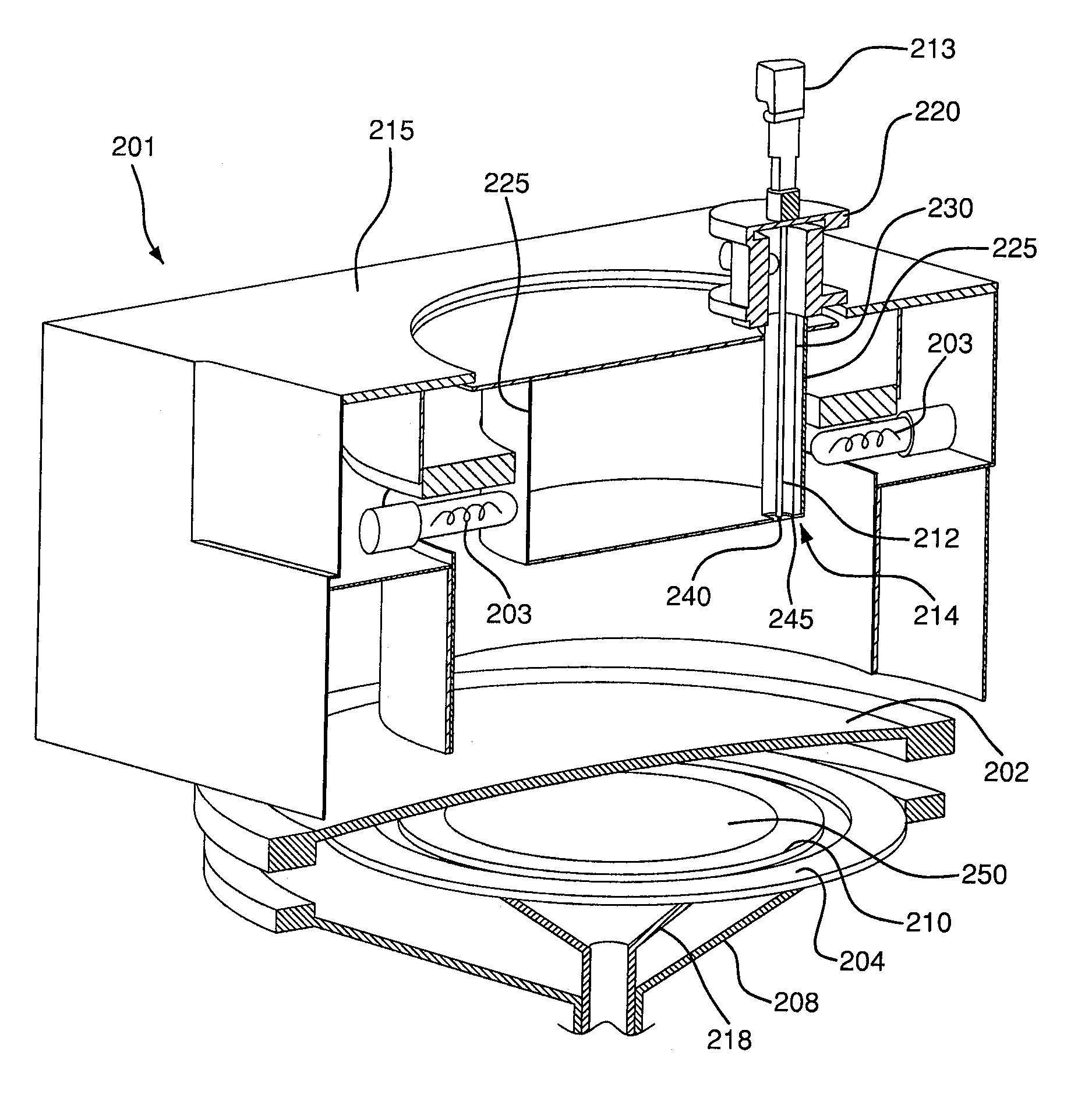
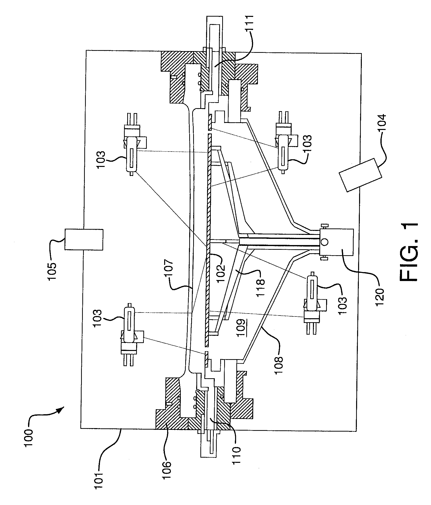
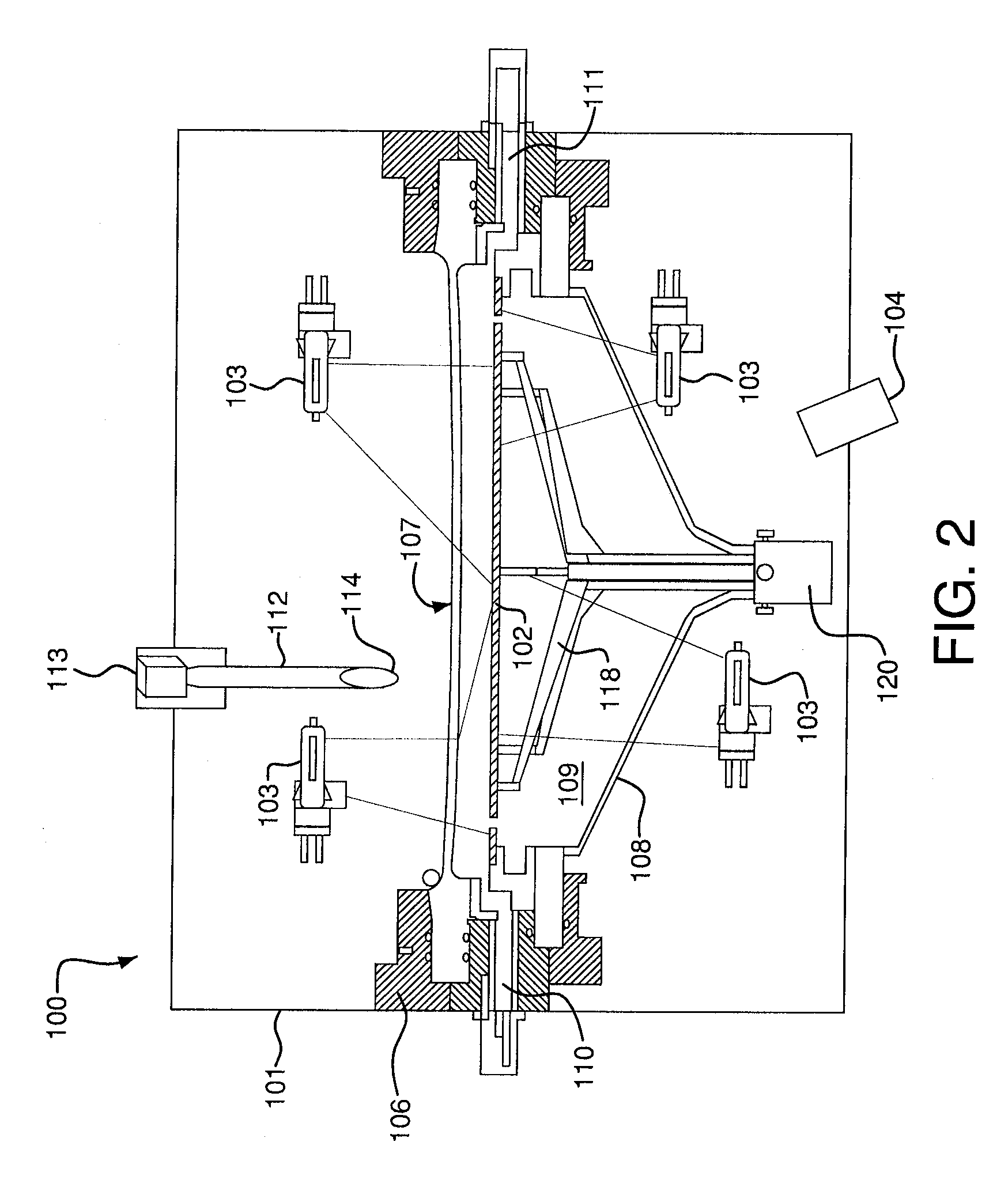
[0033]Semiconductor processing such as epitaxial deposition on a substrate, for example, a wafer utilizes a processing chamber under high temperatures. As used herein, high temperature refers to temperatures exceeding about 500° C., as many semiconductor processes exceed this temperature. For example, many processing temperatures in semiconductor processing chambers are between about 650 and 850° C., and some etching temperatures exceed 1100° C. According to embodiments of the invention, the components of the vision system described herein and located in the process chamber are adapted to withstand such temperatures and still provide wafer and / or susceptor position ...


PUM

PropertyMeasurementUnit
temperatureaaaaaaaaaa

Abstract

A system for monitoring a process inside a high temperature semiconductor process chamber by capturing images is disclosed. Images are captured through a borescope by a camera. The borescope is protected from high temperatures by a reflective sheath and an Infrared (IR) cut-off filter. Images can be viewed on a monitor and can be recorded by a video recording device. Images can also be processed by a machine vision system. The system can monitor the susceptor and a substrate on the susceptor and surrounding structures. Deviations from preferred geometries of the substrate and deviations from preferred positions of susceptor and the substrate can be detected. Actions based on the detections of deviations can be taken to improve the performance of the process. Illumination of a substrate by a laser for detecting deviations in substrate geometry and position is also disclosed.

Description

TECHNICAL FIELD[0001]One or more embodiments of the present invention relate to monitoring a process inside a high temperature semiconductor process chamber. More specifically, embodiments of the invention pertain to a system that utilizes a vision system to monitor the position of the wafer and / or components of the chamber.BACKGROUND[0002]Semiconductor process chambers experience high operational temperatures, for example, in the range of 650-1150° C., in the uniform epitaxial deposition of a material on a substrate such as a wafer. Radiative lamp heating in such chambers and laminar cross-flow design for uniform deposition requires accurate positioning and centering of a wafer in the chamber. A wafer rotation and lift mechanism in the chamber requires extensive set-up for accurate positioning of the wafer during process. During wafer processing, a wafer is positioned on a susceptor. If the susceptor position is incorrect, for example, if it is not level, off-center or exhibits wob...

Claims


Application Information

Patent Timeline
Patent Type & Authority Patents(United States)
IPC IPC(8): G01N21/00G01J5/00B05C11/00C23C16/00
CPCG02B23/2492H01L21/67259H01L21/68714
Inventor PATALAY, KAILASH K.METZNER, CRAIGCARLSON, DAVID K.
Owner APPLIED MATERIALS INC
Why Eureka
Try Eureka