Unlock instant, AI-driven research and patent intelligence for your innovation.

Non-volatile memory device with vertical memory cells

a memory cell and non-volatile technology, applied in the field of semiconductor devices, can solve the problems of difficulty in further increasing the memory density, and the inability to form a single layer of memory cells over a monocrystalline silicon substrate,

Active Publication Date: 2014-06-24
SK HYNIX INC
View PDF2 Cites 0 Cited by
  • Summary
  • Abstract
  • Description
  • Claims
  • Application Information

AI Technical Summary

Benefits of technology

This approach significantly increases memory cell density per unit area, overcoming patterning limitations and reducing production costs by enabling more efficient memory integration.

Problems solved by technology

However, as patterning technology reaches the technical limitation, it is difficult to further increase the memory density.
In such circumstances that there are increased demands for the increase in the memory density, forming a single layer of memory cells over a monocrystalline silicon substrate may not satisfy the demands.

Method used


Image

  • Non-volatile memory device with vertical memory cells
  • Non-volatile memory device with vertical memory cells
  • Non-volatile memory device with vertical memory cells

Examples


first embodiment

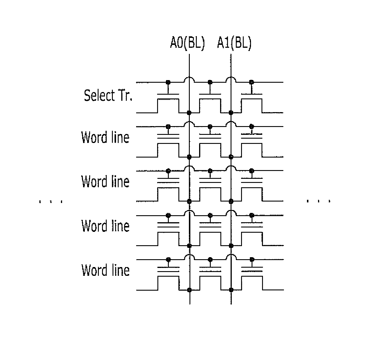
[0025]FIG. 1 is an equivalent circuit diagram of a non-volatile memory device in accordance with the present invention. To be specific, FIG. 1 shows an ORNAND-type flash memory device.

[0026]Referring to FIG. 1, each memory cell is coupled with a word line that functions as a control gate in a memory cell array, and a pair of memory cells shares a common bit line A0 or A1. For example, the memory cell array in the embodiment is coupled with a selection transistor (Tr).

[0027]Depending on how memory cells are coupled with bit lines in response to a word line voltage, the memory cells may write, read, and erase bits of data. Reading a first bit of the data, for example, ‘A’ bit of a memory cell, is carried out by applying the word line voltage and coupling a drain and a source of the memory cell with a bit line A1 and a bit line A0, respectively. Similarly, reading a second bit of the data, for example, ‘B’ bit of a memory cell, is carried out by coupling a drain with a bit line A0 and ...

second embodiment

[0063]FIG. 9 is a plan view illustrating a structure including the junction layers 202A and the cell channel layers 201A in accordance with the present invention. The junction layers 202A and the cell channel layers 201A are coupled with each other. The cell channel layers 201A are penetrated by pillars, i.e., the second insulation layer 105, and a third insulation layer pattern 107A remains between the junction layers 202A.

[0064]Subsequently, selection transistors are formed to select a string of memory cells having a vertical structure. Each selection transistor includes a selection gate 204 and a gate insulation layer 203. In other words, the gate insulation layer 203 surrounding the channels 202B is formed, and then the selection gates 204 are formed. A third insulation layer 205 for inter-layer insulation is formed over each selection gate 204.

[0065]Referring to FIG. 8E, bit lines 206 for applying a current and a voltage are formed over the junction layers 202A.

[0066]FIGS. 10 a...


PUM


Abstract

A non-volatile memory device includes a plurality of gate electrodes stacked over a semiconductor substrate and stretched in a first direction along the semiconductor substrate and a plurality of junction layers having a first region protruding from the semiconductor substrate and crossing the gate electrodes and a second region formed between the gate electrodes.

Description

CROSS-REFERENCE TO RELATED APPLICATIONS[0001]The present application claims priority of Korean Patent Application No. 10-2011-0084122, filed on Aug. 23, 2011, which is incorporated herein by reference in its entirety.BACKGROUND[0002]1. Field[0003]Exemplary embodiments of the present invention relate to a semiconductor device and a fabrication method thereof, and more particularly, to a non-volatile memory device and a fabrication method thereof.[0004]2. Description of the Related Art[0005]When a single layer of memory cells are formed over a monocrystalline silicon substrate, a memory density thereof is determined based on patterning limitation and packaging limitation. The packaging limitation may be relaxed by decreasing the size of patterns so as to increase the memory density.[0006]However, as patterning technology reaches the technical limitation, it is difficult to further increase the memory density. In such circumstances that there are increased demands for the increase in t...

Claims


Application Information

Patent Timeline
Patent Type & Authority Patents(United States)
IPC IPC(8): H01L21/28H01L27/115H01L29/66H01L29/792H10B69/00
CPCH01L29/792H01L27/115H01L29/7926H01L29/66833H01L27/11568H01L21/28282H01L27/11578H01L27/11582H01L29/40117H10B69/00H10B43/20H10B43/30H10B43/27H01L21/823487
Inventor AHN, JUNG-RYUL
Owner SK HYNIX INC