Through silicon via-based oscillator wafer-level-package structure and method for fabricating the same
a technology of silicon via and oscillator, which is applied in the direction of oscillator, semiconductor device details, semiconductor/solid-state device details, etc., can solve the problems of high prior art cost, difficult to reduce package volume, and complicated structure of prior art, so as to reduce cost and ensure stable supply of raw materials
- Summary
- Abstract
- Description
- Claims
- Application Information
AI Technical Summary
Benefits of technology
Problems solved by technology
Method used
Image
Examples
first embodiment
[0048]Refer to FIGS. 4A-4C, which are sectional views schematically showing the process to fabricate the silicon cap according to the present invention.
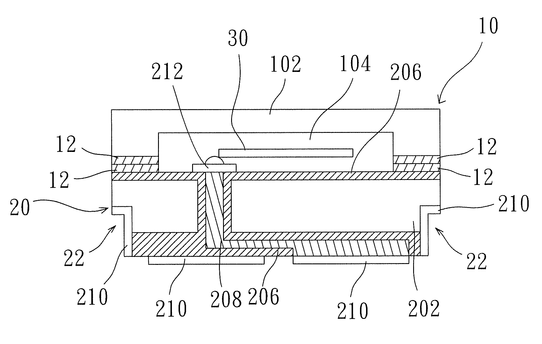
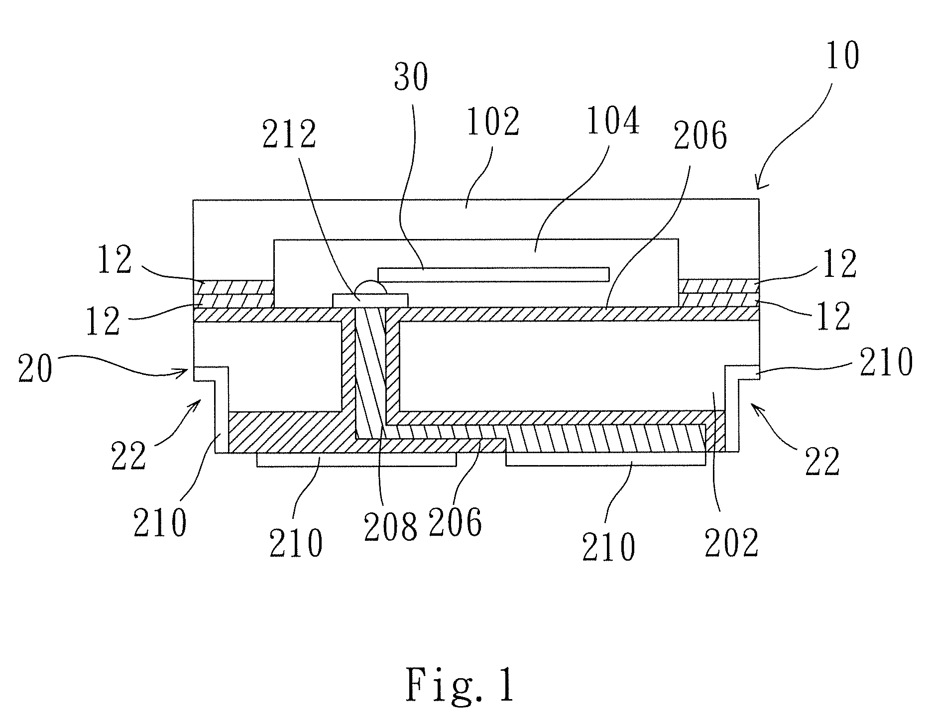
[0049]Firstly, the present invention provides a first silicon wafer 102. Next, form at least one package ring 12 on the lower surface of the first silicon wafer 102. Next, etch the first silicon wafer 102 to form in the first silicon wafer 102 a cavity 102 accommodating an oscillator unit 30. In one embodiment, the etching process may be realized with an ICP (Inductively Coupled Plasma) etching technology, an RIE (Reactive Ion Etching) technology, or a wet etching technology.
[0050]In this embodiment, the package ring 12 is formed on the lower surface of the first silicon wafer 102 to achieve the objective of increasing the airtightness of the oscillator unit 30. In other embodiments of the present invention, the package ring 12 may be alternatively formed on the silicon base 20 to achieve the same objective.
second embodiment
[0051]Refer to FIGS. 4D-4F, which are sectional views schematically showing the process to fabricate the silicon cap according to the present invention. In this embodiment, the silicon cap 10 is fabricated with an alternative method.
[0052]Firstly, the present invention provides a first silicon wafer 102. Next, etch the lower surface of the first silicon wafer 102 to form a cavity 104 on the lower surface of the first silicon wafer 102. Next, electroplate a metal barrier layer 106 on the cavity 104, as shown in FIG. 4F.
[0053]In this embodiment, the present invention uses the electroplated metal barrier layer 106 as the package material (i.e. the package ring) in the succeeding package process. Thereby are saved some conventional process steps. Therefore, the silicon cap 10 can be realized with either of the two aforementioned embodiments.
[0054]Refer to FIGS. 5A-5J, which are sectional views schematically showing the process to fabricate the silicon base according to one embodiment of...
PUM
| Property | Measurement | Unit |
|---|---|---|
| metallic conductive | aaaaa | aaaaa |
| conductive | aaaaa | aaaaa |
| temperature-stable | aaaaa | aaaaa |
Abstract
Description
Claims
Application Information


