Through wiring substrate and manufacturing method thereof

a technology of wiring substrate and manufacturing method, which is applied in the direction of semiconductor/solid-state device details, nuclear engineering, and high-frequency signals, can solve the problems of increased transmission loss of electrical signals, particularly of high-frequency signals, via the through-wire, and poor conductivity, so as to achieve smooth bend parts, the effect of reducing the number of defects and improving the quality of the produ

Inactive Publication Date: 2014-07-22
FUJIKURA LTD
View PDF20 Cites 2 Cited by
  • Summary
  • Abstract
  • Description
  • Claims
  • Application Information

AI Technical Summary

Benefits of technology

[0009]The present invention has been realized in view of the above issues, and aims to provide a through wiring substrate and a manufacturing method thereof that reduce transmission loss of electrical signals such as high-frequency signals, and suppress poor conductivity due to peeling of the electrically-conductive substance from the through-hole.
[0017]According to the invention, it is possible to provide a through wiring substrate, and a manufacturing method thereof, that can reduce transmission loss of electrical signals such as high-frequency signals, and suppress poor conduction due to peeling of the electrically-conductive substance from the through-hole.
[0020]Moreover, when at least one of the outer peripheral part and the inner peripheral part is formed in a circular arc shape, and this circular arc has a radius of curvature within a range of 10 μm to 1000 μm, the bend part is made smoother, whereby poor conduction due to peeling of the electrically-conductive substance can be even further suppressed.
[0021]The through-wire provided in the through wiring substrate of the invention has a bend part. Of the outer peripheral part and the inner peripheral part of the longitudinal cross-section of this bend part, at least the inner peripheral part is a circular arc shape and thus does not have a sharp end part at least in the inner peripheral part. Therefore, local concentration of current to the inner peripheral part is alleviated, and transmission loss of high-frequency signals and the like can be reduced.
[0022]Moreover, when at least one of the outer peripheral part and the inner peripheral part is formed in a circular arc shape, and this circular arc has a radius of curvature within a range of 10 μm to 1000 μm, the bend part is made smoother, whereby transmission loss of high-frequency signals and the like can be further reduced.

Problems solved by technology

When a through-wire provided in a conventional through wiring substrate has a substantially right-angled bend part, there is a problem that current concentrates in the inner peripheral part of the bend part, resulting in increased transmission loss of electrical signals, and in particular of high-frequency signals, via the through-wire.
There is also a problem that an electrically-conductive substance filled by a method such as supercritical film formation method peels away from the through-hole at the sharp end parts of the bend parts, resulting in poor conductivity.

Method used


Image

  • Through wiring substrate and manufacturing method thereof
  • Through wiring substrate and manufacturing method thereof
  • Through wiring substrate and manufacturing method thereof

Examples


first embodiment

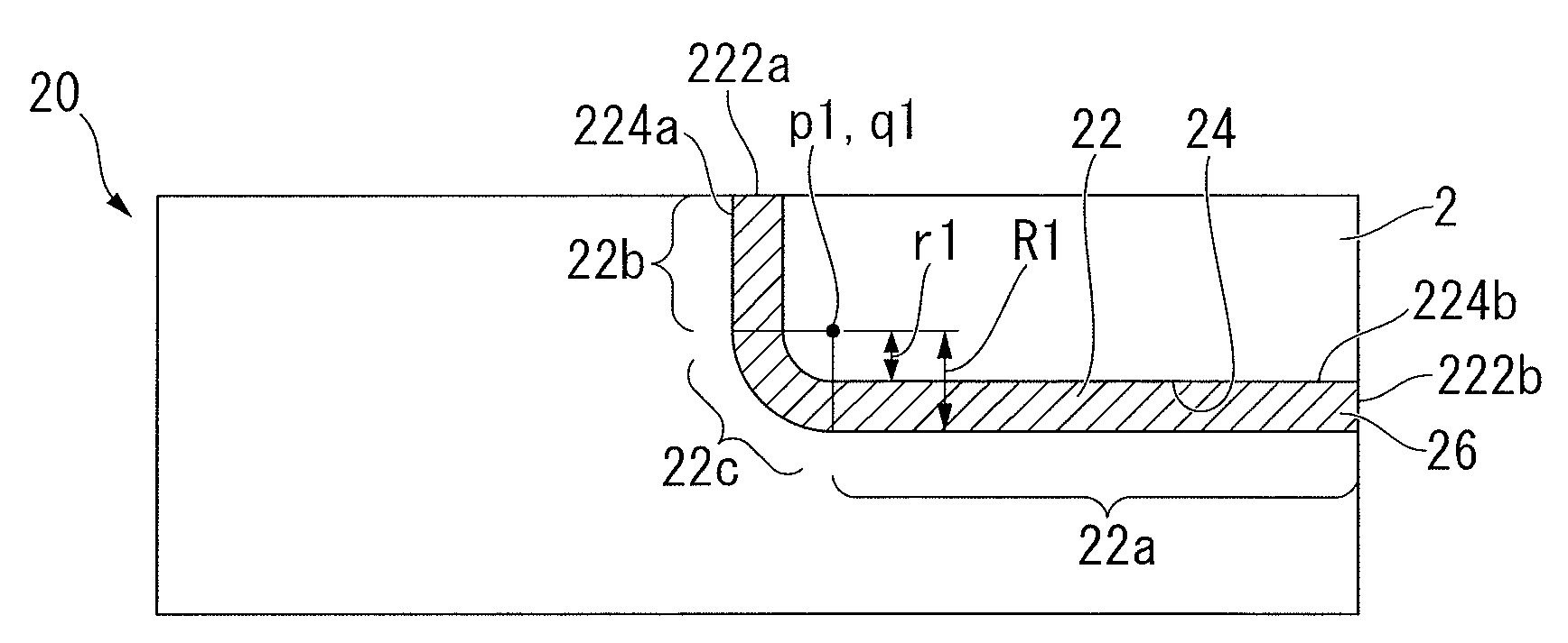
[0035]FIG. 1 is a cross-sectional view of a through wiring substrate 20 according to the invention. The through wiring substrate 20 includes a through-wire 22. The through-wire 22 is formed by providing a through-hole 24 that penetrates between one face (a top face or a bottom face; first face) constituting a single substrate 2 and one side face (second face), and filling, or forming a film of, an electrically-conductive substance 26 into this through-hole 24. The through-hole 24 has a bend part (curved part) 22c. The outer peripheral part and inner peripheral part of the longitudinal cross-section of this bend part 22c are formed in a circular arc shape. As shown in FIG. 1, this bend part, in the longitudinal cross-section, includes an inner peripheral part that is curved in a recessed shape, and an outer peripheral part that is curved in a protruding shape. The through-hole 24 includes a linear part 22b, the bend part 22c, and a linear part 22a, which are continuously disposed. Th...

second embodiment

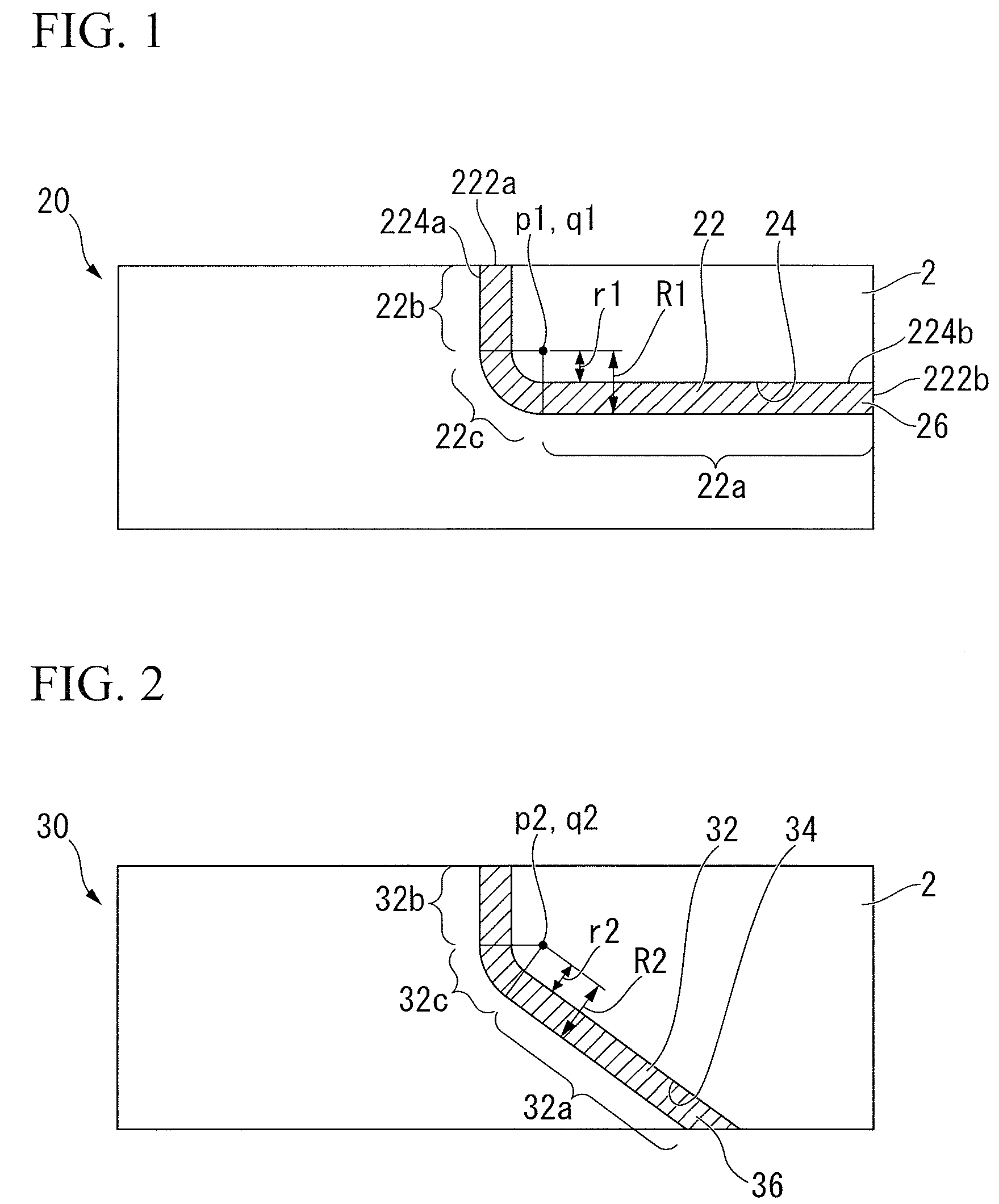
[0045]FIG. 2 is a cross-sectional view of a through wiring substrate 30 according to the invention. The through wiring substrate 30 includes a through-wire 32, which is formed by providing a through-hole 34 that penetrates between one face (a top face or a bottom face; first face) and another face (a bottom face or a top face; second face) constituting a single substrate 2, and filling, or forming a film of, an electrically-conductive substance 36 in this through-hole 34. The through-hole 34 has a bend part (curved part) 32c, and the outer peripheral part and inner peripheral part of the longitudinal cross-section of the bend part 32c are formed in a circular arc shape.

[0046]The cross-section of the through wiring substrate 30 of FIG. 2 is a longitudinal cross-section along the center line of the through-wire 32. One end of the through-wire 32 is a first conductive part exposed at one face (first face) of the through wiring substrate 30. A linear part 32b extends from one end of the...

third embodiment

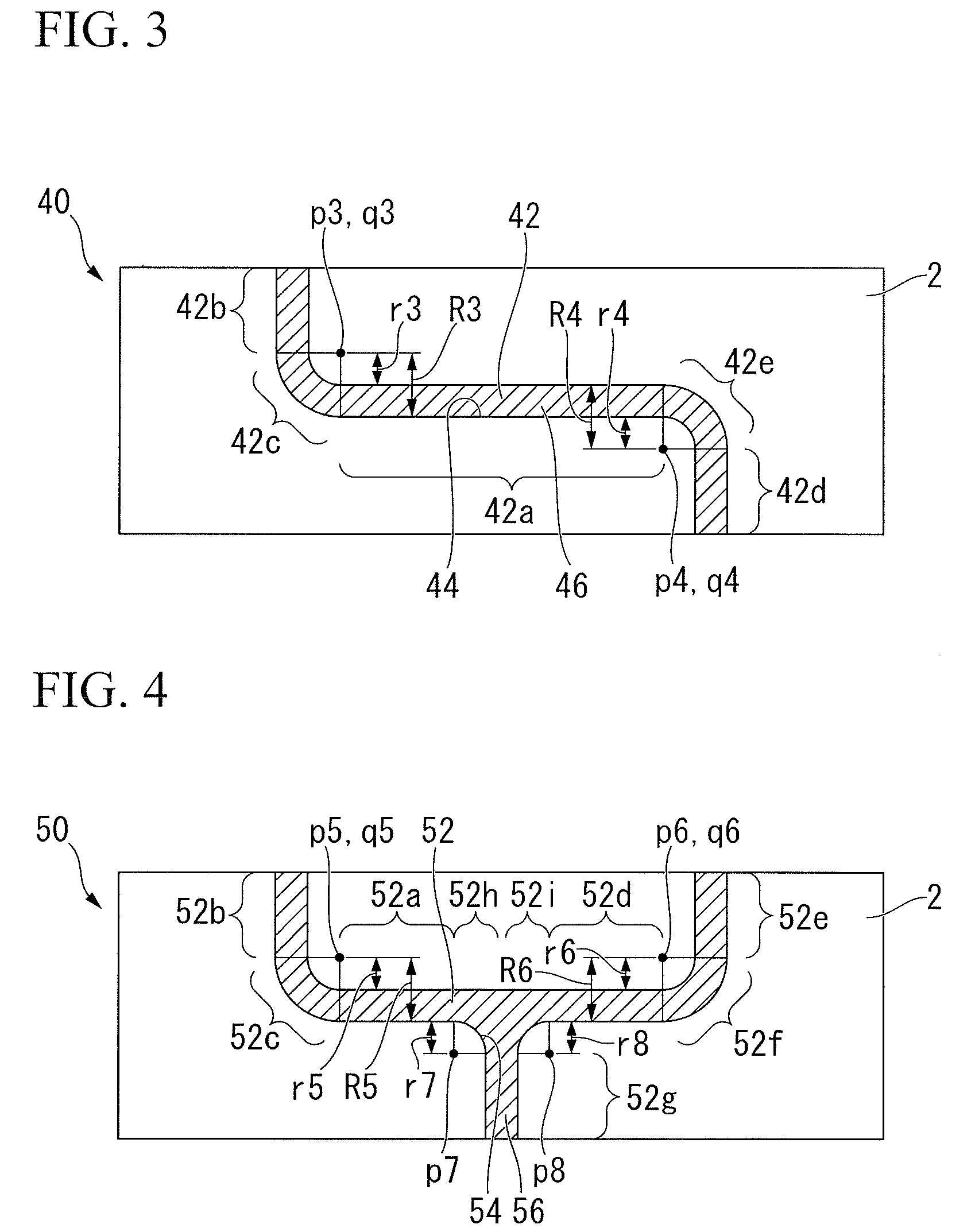
[0055]FIG. 3 is a cross-sectional view of a through wiring substrate 40 according to the invention. The through wiring substrate 40 includes a through-wire 42, which is formed by providing a through-hole 44 that penetrates between one face (a top face or a bottom face; first face) and another face (a bottom face or a top face; second face) constituting a single substrate 2, and filling, or forming a film of, an electrically-conductive substance 46 in this through-hole 44. The through-hole 44 has a first bend part 42c and a second bend part 42e. The outer peripheral part and inner peripheral part of the longitudinal cross-section of the first bend part 42c, and the outer peripheral part and the inner peripheral part of the longitudinal cross-section of the second bend part 42e are each formed in a circular arc shape. In other words, the through-wire includes the first bend part 42c and the second bend part 42e, and the outer peripheral parts and inner peripheral parts of the first be...


PUM


Abstract

A through wiring substrate includes a substrate having a first face and a second face; and a through-wire formed by filling, or forming a film of, an electrically-conductive substance into a through-hole, which penetrates between the first face and the second face. The through-hole has a bend part comprising an inner peripheral part that is curved in a recessed shape and an outer peripheral part that is curved in a protruding shape, in a longitudinal cross-section of the through-hole, and at least the inner peripheral part is formed in a circular arc shape in the longitudinal cross-section.

Description

CROSS REFERENCE TO RELATED APPLICATIONS[0001]This application is a continuation application based on a PCT Patent Application No. PCT / JP2010 / 004139, filed Jun. 22, 2010, whose priority is claimed on Japanese Patent Application No. 2009-159869 filed Jul. 6, 2009, the entire content of which is hereby incorporated by reference.BACKGROUND OF THE INVENTION[0002]1. Field of the Invention[0003]The present invention relates to a through wiring substrate that has a through-wire which penetrates the interior of a substrate (interposer substrate with through-hole interconnection) and a manufacturing method thereof.[0004]2. Description of the Related Art[0005]Conventionally, a method of providing a through-wire that penetrates the interior of a substrate (through-hole interconnection) is used as a method of electrically connecting a first device, mounted on a first face which is one face of the substrate, to a second device, mounted on a second face which is another face of the substrate. The ...

Claims


Application Information

Patent Timeline
Patent Type & Authority Patents(United States)
IPC IPC(8): H05K1/11H05K1/00
CPCH05K3/101H01L23/15H01L23/473H01L23/49827H01L2924/0002H01L2924/09701H05K1/0272H05K3/4053H05K2201/09272H01L2924/00
Inventor YAMAMOTO, SATOSHIHASHIMOTO, HIROKAZU
Owner FUJIKURA LTD
Why Eureka
Try Eureka