Light emitting diode, manufacturing method thereof, light emitting diode module, and manufacturing method thereof

a technology of light-emitting diodes and manufacturing methods, which is applied in the manufacturing of semiconductor/solid-state devices, semiconductor devices, electrical devices, etc., can solve the problems of inapplicability of led to products, inability to obtain uniform white light, and increase the non-uniformity of color distribution, so as to achieve uniform wavelength conversion characteristics, increase productivity per unit time, and low color distribution non-uniformity

Active Publication Date: 2014-07-22
SAMSUNG ELECTRONICS CO LTD
View PDF10 Cites 9 Cited by
  • Summary
  • Abstract
  • Description
  • Claims
  • Application Information

AI Technical Summary

Benefits of technology

[0016]Another aspect of the present invention provides an LED, a manufacturing method of the LED, an LED module, and a manufacturing method of the LED module, achieving uniform wavelength conversion characteristics and low non-uniformity of color distribution by employing a phosphor pre-form.
[0017]Still another aspect of the present invention provides an LED, a manufacturing method of the LED, an LED module, and a manufacturing method of the LED module, increasing productivity per unit time by employing a phosphor pre-form.

Problems solved by technology

However, in the foregoing conventional methods, uniform white light may not be obtained since the phosphor resin is applied non-uniformly.
When uniformity of the phosphor resin is extremely low, non-uniformity of color distribution may be so increased that the LED may be inapplicable to products.
As a result, yield may be affected.
A structure that modularizes the LED package by mounting the LED package on a printed circuit board (PCB) may have a limit to miniaturization of an LED module, and may not decrease a price of the LED module due to a high error rate during at least two mounting processes.
However, the foregoing method has a difficulty in manufacturing the LED chip providing a white light and has a limit to decrease of color dispersion in an LED package level.

Method used


Image

  • Light emitting diode, manufacturing method thereof, light emitting diode module, and manufacturing method thereof
  • Light emitting diode, manufacturing method thereof, light emitting diode module, and manufacturing method thereof
  • Light emitting diode, manufacturing method thereof, light emitting diode module, and manufacturing method thereof

Examples


Embodiment Construction

[0055]Reference will now be made in detail to exemplary embodiments of the present invention, examples of which are illustrated in the accompanying drawings, wherein like reference numerals refer to the like elements throughout. In the description of the present invention, if detailed descriptions of a related disclosed art or configurations are determined to unnecessarily make the subject matter of the present invention obscure, they will be omitted. Terms to be used below are defined based on their functions in the present invention and may vary according to users, user's intentions, or practices. Therefore, the definitions of the terms should be determined based on the entire specification.

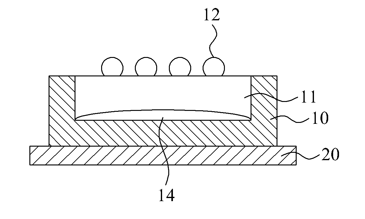
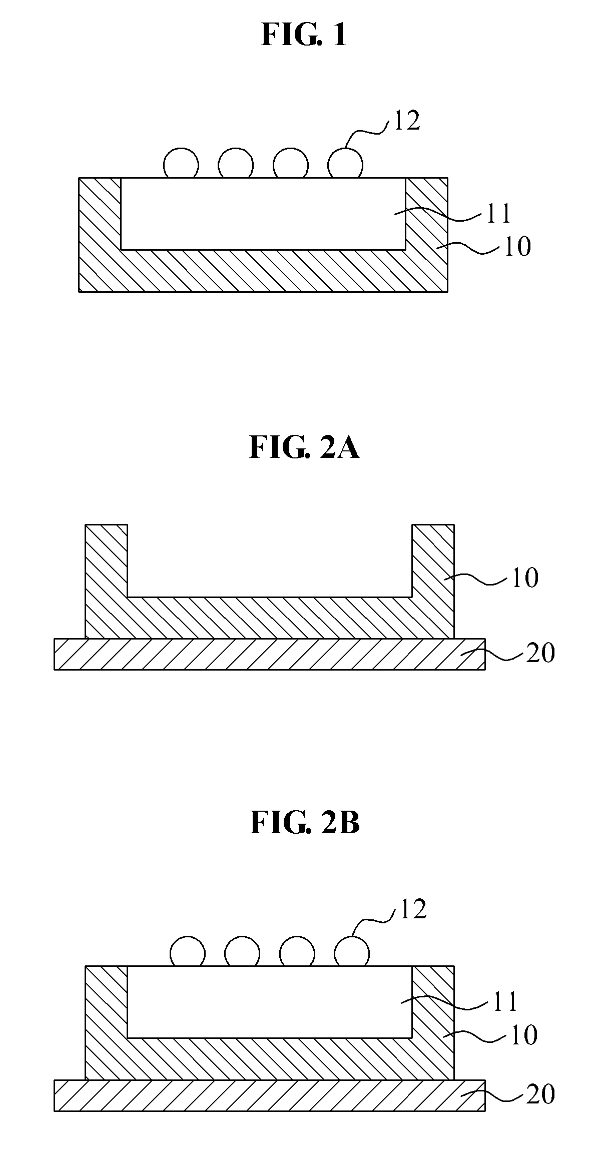
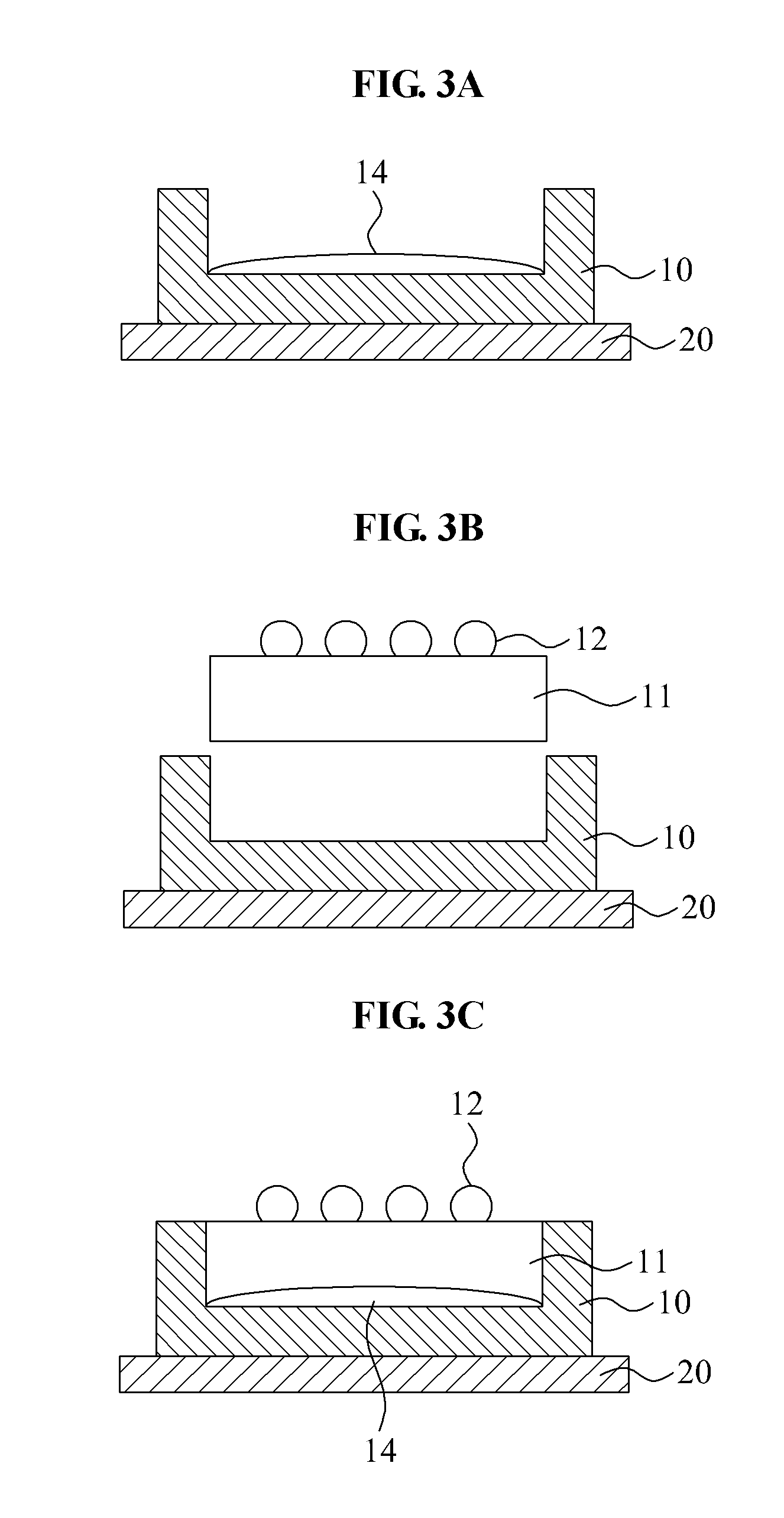
[0056]FIG. 1 is a cross-sectional view of a light emitting diode (LED) according to an embodiment of the present invention. Referring to FIG. 1, the LED according to the embodiment of the present invention may include a phosphor mold 10 including a phosphor particle and a transparent resin and ...


PUM


Abstract

A manufacturing method of a light emitting diode (LED) and a manufacturing method of an LED module are provided. The manufacturing method of the LED may include manufacturing a plurality of LED chips, manufacturing a phosphor pre-form including a plurality of mounting areas for mounting the plurality of LED chips, applying an adhesive inside the phosphor pre-form, mounting each of the plurality of LED chips in each of the plurality of mounting areas, and cutting the phosphor pre-form to which the plurality of LED chips are mounted, into units including individual LED chips.

Description

CROSS-REFERENCE TO RELATED APPLICATION[0001]This application claims the benefit of Korean Patent Applications No. 10-2011-0104223, filed on Oct. 12, 2011, No. 10-2011-0027021, filed on Mar. 25, 2011, and No. 10-2011-0027033 filed on Mar. 25, 2011, in the Korean Intellectual Property Office, the disclosure of which is incorporated herein by reference.BACKGROUND[0002]1. Field of the Invention[0003]The present invention relates to a light emitting diode (LED) having uniform wavelength conversion characteristics, a manufacturing method of the LED, an LED module, and a manufacturing method of the LED module.[0004]2. Description of the Related Art[0005]A light emitting diode (LED) chip is a semiconductor device that converts electrical energy to optical energy. The LED chip includes a compound semiconductor generating light having a particular wavelength according to an energy band gap. Use of LEDs is expanding to a field of displays such as a mobile display and a computer monitor, a fiel...

Claims


Application Information

Patent Timeline
Patent Type & Authority Patents(United States)
IPC IPC(8): H01L33/00
CPCH01L2933/0041H01L33/505H01L33/62H01L2224/32245H01L2224/48091H01L2224/73265H01L2224/16227H01L2924/15153H01L2224/73267H01L2224/97H01L2224/04105H01L21/568H01L2224/92144H01L2224/32225H01L2224/12105H01L2924/00014H01L2224/83
Inventor KIM, HAK HWANKIM, MIN JUNGMOON, KYUNG MISONG, JONG SUPYOU, JAE SUNGCHOI, ILL HEOUNGYOO, CHEOL JUN
Owner SAMSUNG ELECTRONICS CO LTD
Why Eureka
Try Eureka