
Memory system and operating method thereof

a memory system and operating method technology, applied in the field of memory system and operating method thereof, can solve the problems of data loss when the power is turned off and difficulty in updating the contents of the memory

Inactive Publication Date: 2014-08-19
SAMSUNG ELECTRONICS CO LTD
View PDF49 Cites 27 Cited by
  • Summary
  • Abstract
  • Description
  • Claims
  • Application Information

AI Technical Summary

Benefits of technology

This approach enhances data reliability and reduces the time and power required for error correction by enabling on-device correction of errors, thereby improving operational efficiency and reducing resource utilization.

Problems solved by technology

In both SRAM and DRAM devices, data remains stored and may be read as long as the power is applied, but data is lost when the power is turned off.
Mask Read-Only Memory (MROM), Programmable Read-Only Memory (PROM) and Erasable Programmable Read-Only Memory (EPROM) nonvolatile memory devices are not free to erase and write by system itself, so it is not easy to update the contents of the memory.

Method used


Image

  • Memory system and operating method thereof
  • Memory system and operating method thereof
  • Memory system and operating method thereof

Examples


Embodiment Construction

[0082]Reference will now be made in detail to the embodiments of the present general inventive concept, examples of which are illustrated in the accompanying drawings, wherein like reference numerals refer to the like elements throughout. The embodiments are described below in order to explain the present general inventive concept while referring to the figures. This inventive concept may, however, be embodied in many different forms and should not be construed as limited to the embodiments set forth herein. Rather, these embodiments are provided so that this disclosure will be thorough and complete, and will fully convey the scope of the inventive concept to those skilled in the art. In the drawings, the size and relative sizes of layers and regions may be exaggerated for clarity. Like numbers refer to like elements throughout.

[0083]It will be understood that, although the terms first, second, third etc. may be used herein to describe various elements, components, regions, layers a...


PUM


Abstract

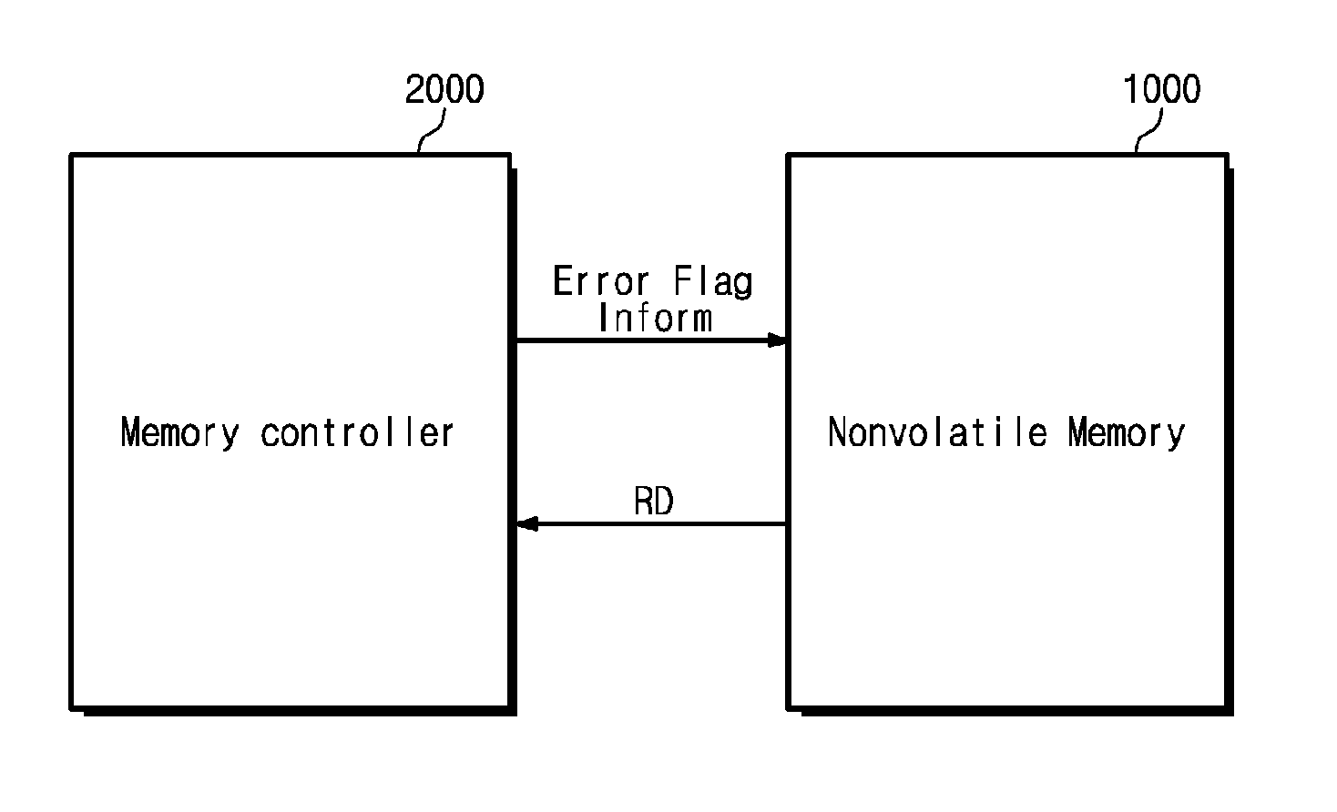
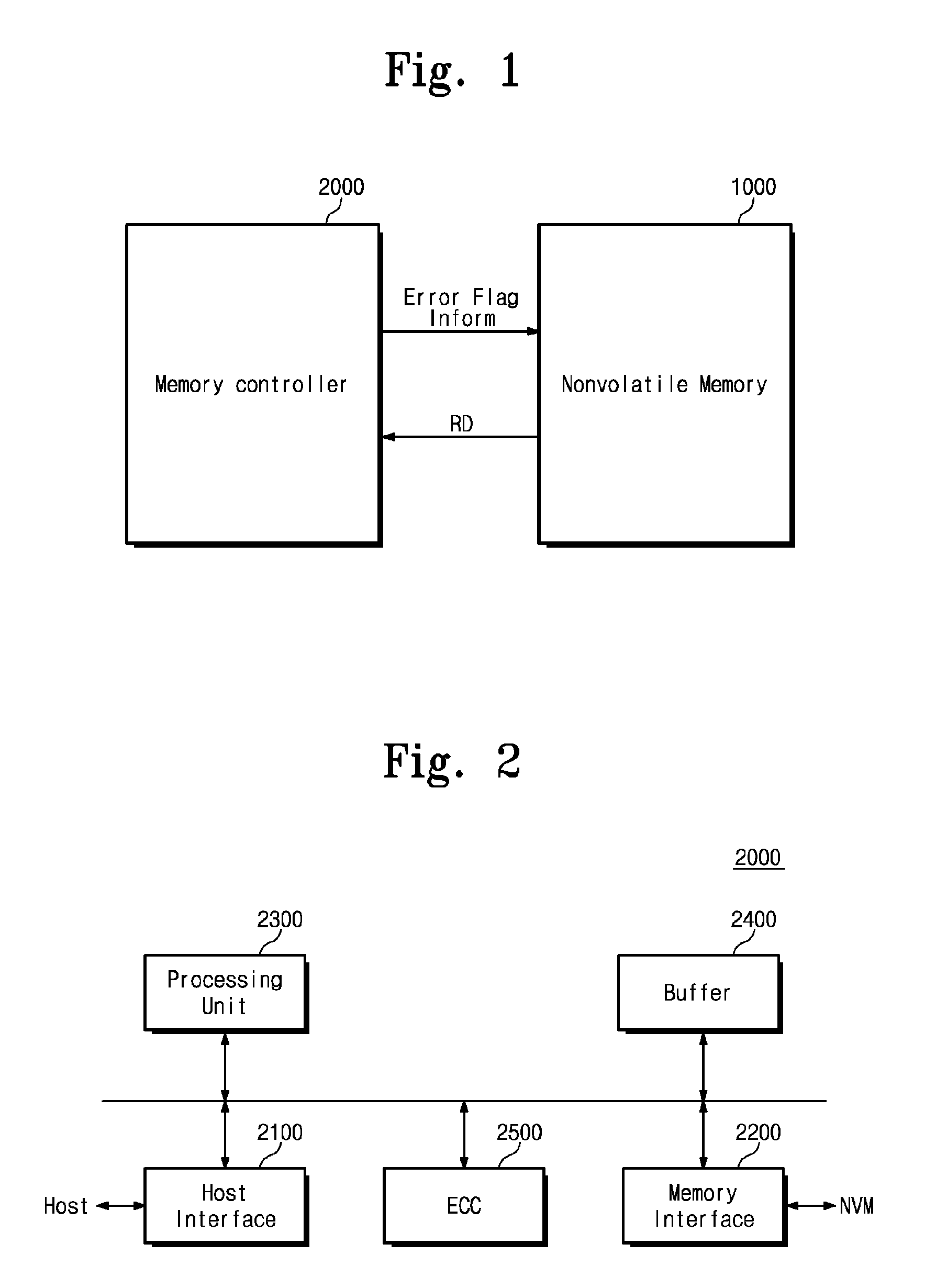
A memory system includes a nonvolatile memory device and a memory controller configured to control the nonvolatile memory device and configured to provide the nonvolatile memory device with error flag information including error location information of an error of data read from the nonvolatile memory device.

Description

CROSS-REFERENCE TO RELATED APPLICATIONS[0001]This application claims the benefits of priority, under 35 U.S.C §119, from Korean Patent Application No. 10-2011-0114282 filed on Nov. 4, 2011, the entirety of which is incorporated by reference herein.BACKGROUND OF THE INVENTION[0002]1. Field of the Invention[0003]Exemplary embodiments relate to a memory system including a nonvolatile memory device and a controller to control the nonvolatile memory.[0004]2. Description of the Related Art[0005]Semiconductor memory devices are a vital microelectronic component commonly found in digital logic systems, such as computers, and microprocessor-based applications ranging from satellites to consumer electronics. Therefore, advances in the fabrication of semiconductor memory devices, including process enhancements and circuit-design-related developments that allow scaling to higher memory densities and faster operating speeds, help establish performance standards for other digital logic families.[...

Claims


Application Information

Patent Timeline
Patent Type & Authority Patents(United States)
IPC IPC(8): G11C8/00G11C11/34G06F11/10H03M13/00G06F11/00H03M13/15G06F11/08G11C29/00
CPCG06F11/1016G06F11/1008G06F11/08G06F11/10G06F11/1048G06F11/1068G06F11/1076G06F11/108H03M13/151H03M13/1525H03M13/1545G11C11/5628G11C16/3418G11C16/10G11C16/06G11C16/26G11C16/34
Inventor JOO, SANG-HYUNPARK, KITAEYOON, SANGYONGHAN, JINMAN
Owner SAMSUNG ELECTRONICS CO LTD
Learn More