Semiconductor device and driving method the same
a technology of semiconductor devices and driving methods, applied in the direction of memory adressing/allocation/relocation, instruments, digital storage, etc., can solve the problems of confusion in the place where such a memory is really used, complicated procedures, etc., to prevent miswriting and tampering data, reduce the occurrence of causing defects such as writing defects, and improve the reliability of wireless communication between the rfid tag and the communication device or the lik
- Summary
- Abstract
- Description
- Claims
- Application Information
AI Technical Summary
Benefits of technology
Problems solved by technology
Method used
Image
Examples
embodiment 1
[0062]In this embodiment, a configuration of a semiconductor device of one embodiment of the present invention that is capable of communicating data through wireless communication will be described.
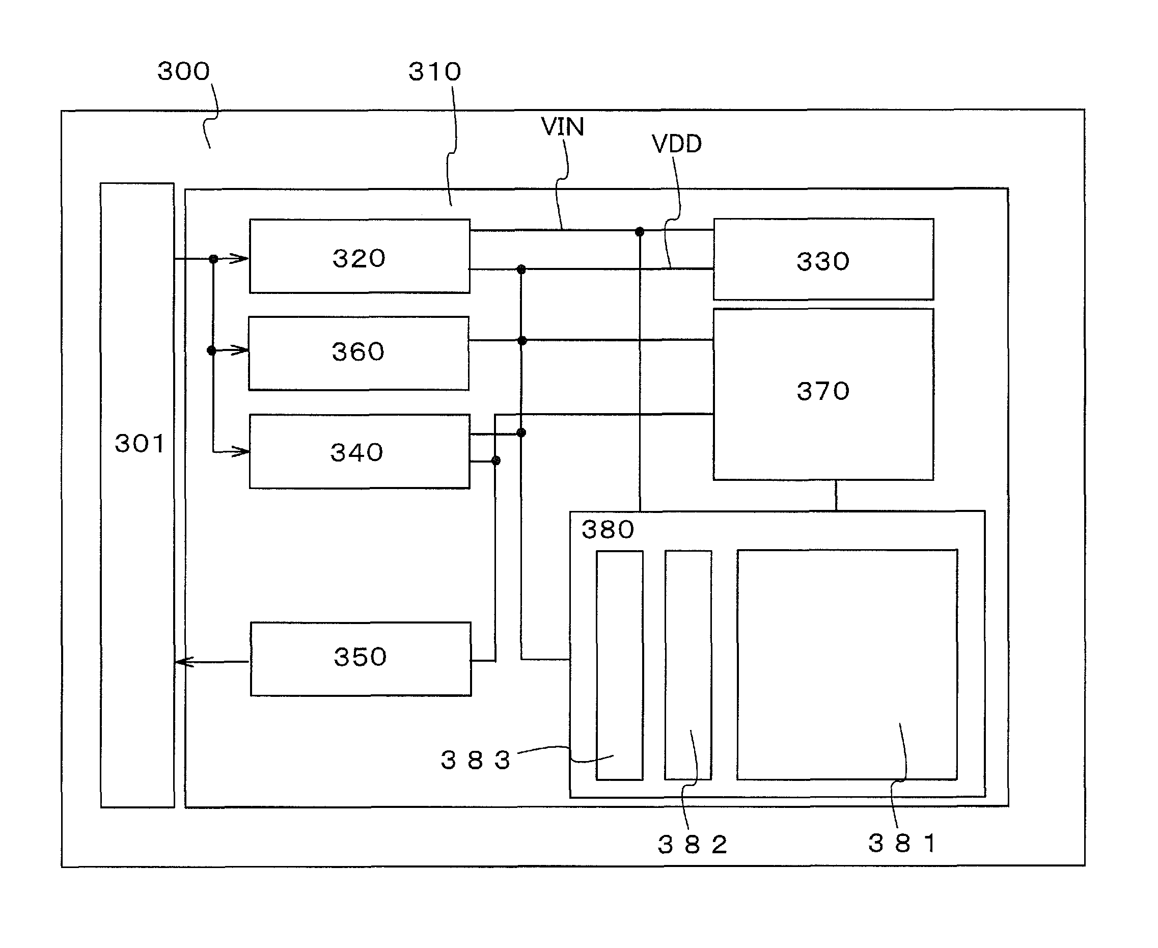
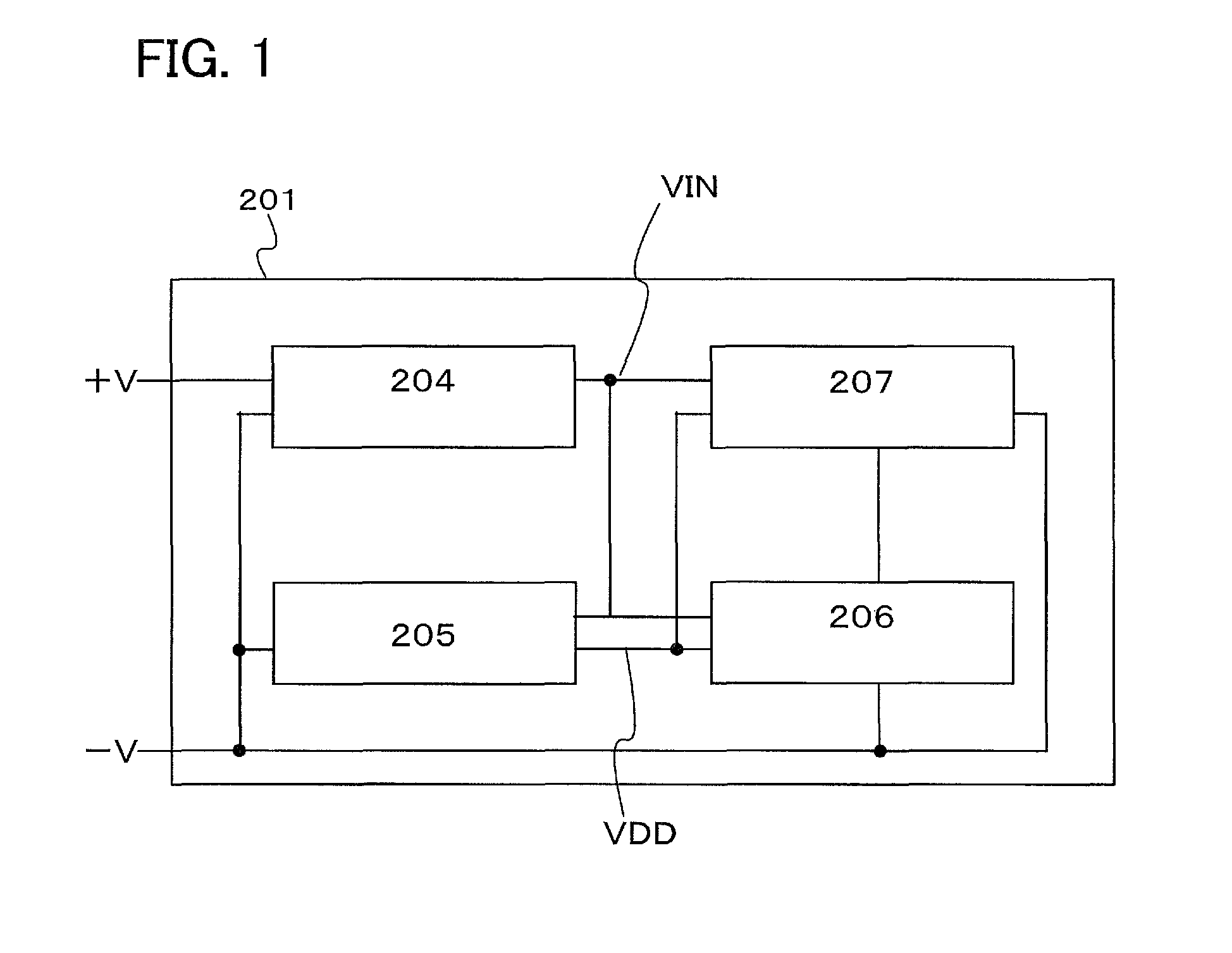
[0063]As illustrated in FIG. 1, a semiconductor device 201 includes an input circuit 204, a circuit 205 which generates a constant voltage, a control circuit 206, and an OTP memory or write-once memory (hereinafter referred to as a memory) 207. In this embodiment, an RFID tag using the semiconductor device 201 in FIG. 1 will be described with reference to FIG. 3. As illustrated in FIG. 3, the case where a memory 380 includes an information sector 381 and a sector for preventing additional writing 382 is described. The information sector 381 and the sector for preventing additional writing 382 are electrically connected to each other.
[0064]An input circuit 320 rectifies an input AC signal to generate a DC voltage. Any circuit configuration can be employed as long as the circuit rectifies a...
embodiment 2
[0081]In this embodiment, a structure of a semiconductor device of one embodiment of the present invention which can perform data communication through wireless communication and which is different from the structure described in Embodiment 1 will be described.
[0082]As illustrated in FIG. 1, the semiconductor device 201 includes the input circuit 204, the circuit 205 which generates a constant voltage, the control circuit 206, and the memory 207. In Embodiment 2, an RFID tag using the semiconductor device 201 in FIG. 1 will be described with reference to FIG. 4. As illustrated in FIG. 4, the case where the memory 380 includes the information sector 381, the sector for preventing additional writing 382, and a sector for determining whether writing is possible 383 is described. A semiconductor integrated circuit illustrated in FIG. 4 is the same as the semiconductor integrated circuit described in Embodiment 1 except the structure of the memory. Note that the information sector 381, t...
embodiment 3
[0101]In this embodiment, a structure and operation of a semiconductor device of one embodiment of the present invention when it is provided for an RFID tag will be described.
[0102]A schematic view of a wireless communication system is illustrated in FIG. 9. The wireless communication system mainly includes a communication device 3010, an antenna unit 3020 which is electrically connected to the communication device 3010, an RFID tag 300, and a controlling terminal 3030 which controls the communication device.
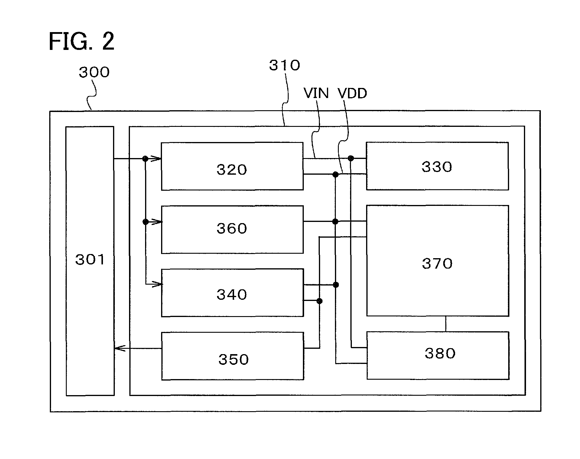
[0103]A circuit configuration of the RFID tag 300 is illustrated in FIG. 2. The RFID tag 300 includes an antenna 301 and the semiconductor integrated circuit 310. Although not illustrated, the antenna 301 may be provided in the semiconductor integrated circuit 310 or may be provided outside the semiconductor integrated circuit 310 as illustrated in FIG. 2. The semiconductor integrated circuit 310 includes the input circuit 320, the circuit 330 which generates a constant voltage,...
PUM
 Abstract
Description
Claims
Application Information


