Supercharge Your Innovation With Domain-Expert AI Agents!

Organic light emitting display device capable of compensating threshold voltage of a driving transistor and driving method thereof

a display device and driving transistor technology, applied in the direction of electric digital data processing, instruments, computing, etc., can solve the problems of difficult manufacturing of the transistors used in each of the pixels, non-uniform display luminance, and varying current flow to the organic light emitting diode, so as to reduce manufacturing costs and simplify the structure

Active Publication Date: 2014-09-09
SAMSUNG DISPLAY CO LTD
View PDF17 Cites 9 Cited by
  • Summary
  • Abstract
  • Description
  • Claims
  • Application Information

AI Technical Summary

Benefits of technology

The invention allows for faster driving of a display device by compensating for the threshold voltage of the driving transistor. Additionally, the device can be driven in both simultaneous emission and non-emission schemes, which simplifies the structure and reduces manufacturing costs.

Problems solved by technology

A disadvantage of such an organic light emitting display device is that the amount of current that flows to the organic light emitting diode varies depending on a threshold voltage of the driving transistor provided in each of the pixels.
It is difficult to manufacture the transistors used in each of the pixels in the organic light emitting display device to have the same characteristics given the current processing technology.
This results in variability in the threshold voltage of the driving transistors in each of the pixels, which causes a non-uniform display luminance.
However, in the case of high-speed driving at 120 Hz or more, a charging duration of the threshold voltage of the driving transistor is shortened, such that compensation of the threshold voltage of the driving transistor may become impossible.

Method used


Image

  • Organic light emitting display device capable of compensating threshold voltage of a driving transistor and driving method thereof
  • Organic light emitting display device capable of compensating threshold voltage of a driving transistor and driving method thereof
  • Organic light emitting display device capable of compensating threshold voltage of a driving transistor and driving method thereof

Examples


first embodiment

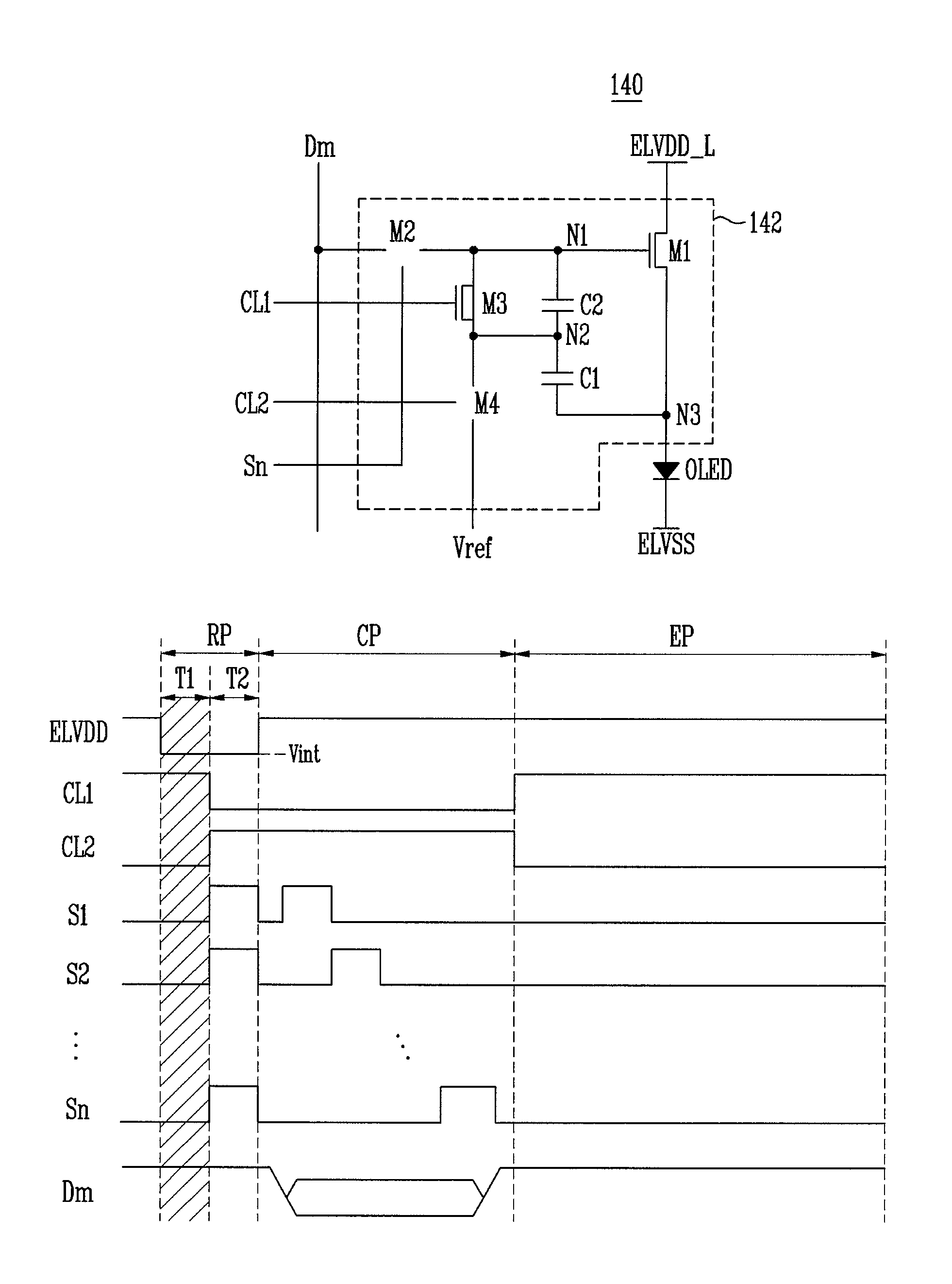
[0046]FIG. 3 is a diagram showing a pixel 140 according to the present invention. In FIG. 3, the pixel 140 connected to the n-th scan line Sn and the m-th data line Dm is shown for convenience of description.

[0047]Referring to FIG. 3, the pixel 140 according to the first embodiment of the present invention includes the organic light emitting diode OLED and a pixel circuit 142 that is connected to the data line Dm, the scan line Sn, the first control line CL1, and the second control line CL2. Each of the data line Dm, the scan line Sn, the first control line C11, and the second control line CL2 contribute to the control of the organic light emitting diode OLED.

[0048]An anode electrode of the organic light emitting diode OLED is connected to the pixel circuit 142, and a cathode electrode of the organic light emitting diode OLED is connected to the second ELVSS. The organic light emitting diode OLED emits light having a luminance that is determined by a current supplied from the pixel ...

second embodiment

[0066]FIG. 5 is a diagram showing a pixel according to the present invention. When FIG. 5 is described, the same reference numerals refer to the same components as those of FIG. 3 and a detailed description thereof will be omitted.

[0067]Referring to FIG. 5, a pixel 140 according to the second embodiment of the present invention includes a pixel circuit 142′ and an organic light emitting diode OLED. Herein, a first electrode of a fourth transistor M4 included in the pixel circuit 142′ is connected to a first power ELVDD and the rest of the components are established similarly as the pixel shown in FIG. 3.

[0068]When the first electrode of the fourth transistor M4 is connected to the first power ELVDD, voltage levels of a first high power ELVDD_H, a first low power ELVDD_L, and a data signal voltage Vdata are set as shown in Equation 4.

ELVDD—H≧Vdata>ELVDD—L  Equation 4

[0069]Referring to Equation 4, the data signal voltage Vdata is set to a voltage equal to or lower than the first high ...

third embodiment

[0070]FIG. 6 is a diagram showing a pixel according to the present invention. When FIG. 6 is described, the same reference numerals refer to the same components as those of FIG. 3 and a detailed description thereof will not be provided again. In addition, a pixel 140 connected to an n-th scan line Sn and an m-th data line Dm is shown for convenience of description.

[0071]Referring to FIG. 6, the pixel 140 according to the third embodiment of the present invention includes an organic light emitting diode OLED and a pixel circuit 142″.

[0072]The pixel circuit 142″ is connected between a third node N3 and an initial voltage Vint and includes a fifth transistor M5 that is switched on when a scan signal is supplied to an n−1 scan line Sn−1. When the fifth transistor M5 is switched on, initial voltage Vint is supplied to the third node N3. In this case, the voltage of the first power ELVDD maintains the voltage of the high level during a frame period. The voltage level including the initial...


PUM


Abstract

An organic light emitting display device includes: a plurality of pixels at crossing regions of a plurality of scan lines and data lines; a first control line and a second control line commonly connected with the plurality of pixels; a control line driver configured to supply a first control signal to the first control line and a second control signal to the second control line, where the second control signal is not concurrent with the first control signal; and a first power supply that supplies a first power to each of the plurality of pixels, where a voltage level of the first power is configured to change at least once during a frame period for each of the pixels.

Description

CROSS-REFERENCE TO RELATED APPLICATIONS[0001]This application claims priority to and the benefit of Korean Patent Application No. 10-2009-0099214, filed in the Korean Intellectual Property Office on Oct. 19, 2009, the entire content of which is incorporated herein by reference.BACKGROUND[0002]1. Field[0003]The embodiment of the present invention relates to an organic light emitting display device and a driving method thereof.[0004]2. Description of Related Art[0005]In recent years, various flat panel display devices with reduced weight and volume in comparison to a cathode ray tube have been developed. Examples of the flat panel display devices include a liquid crystal display device, a field emission display device, a plasma display panel, and an organic light emitting display device.[0006]An organic light emitting display device displays images by using organic light emitting diodes that emit light by recombination of electrons and holes. Such an organic light emitting display dev...

Claims


Application Information

Patent Timeline
Patent Type & Authority Patents(United States)
IPC IPC(8): G09G5/00G06F3/038G09G3/32
CPCG09G3/3233G09G2320/043G09G2300/0819G09G2310/0262G09G2300/0852G09G2310/0251G09G3/20G09G3/30
Inventor CHOI, SANG-MOOKANG, CHUL-KYU
Owner SAMSUNG DISPLAY CO LTD
Features
  • R&D
  • Intellectual Property
  • Life Sciences
  • Materials
  • Tech Scout
  • Unparalleled Data Quality
  • Higher Quality Content
  • 60% Fewer Hallucinations
Learn More