

Dynamically tracking spectrum features for endpoint detection
a spectrum feature and dynamic tracking technology, applied in the field of optical monitoring, can solve problems such as difficulty in tracking the selected spectrum feature, and achieve the effect of reducing processing resources
- Summary
- Abstract
- Description
- Claims
- Application Information
AI Technical Summary
Benefits of technology
Problems solved by technology
Method used
Image

Examples
Embodiment Construction
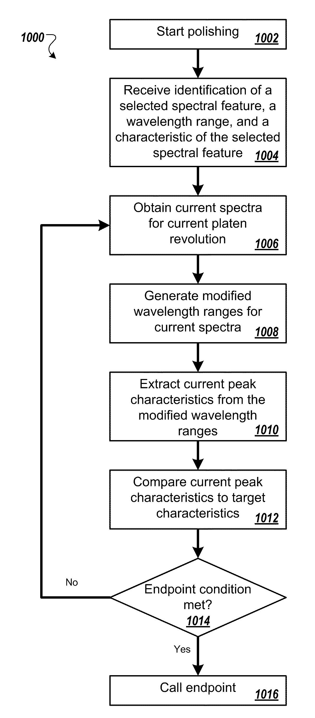
[0032]One optical monitoring technique is to measure spectra of light reflected from a substrate during polishing, and identify a matching reference spectra from a library. One potential problem with the spectrum matching approach is that for some types of substrates there are significant substrate-to-substrate differences in underlying die features, resulting in variations in the spectra reflected from substrates that ostensibly have the same outer layer thickness. These variations increase the difficulty of proper spectrum matching and reduce reliability of the optical monitoring.
[0033]One technique to counteract this problem is to measure spectra of light reflected off of substrates being polished and identify changes in spectral feature characteristics. Tracking changes in a characteristic of a feature of the spectrum, e.g., a wavelength of a spectral peak, can allow greater uniformity in polishing between substrates within a batch. By determining a target difference in the spec...
PUM
| Property | Measurement | Unit |
|---|---|---|
| wavelength range | aaaaa | aaaaa |
| wavelength range | aaaaa | aaaaa |
| width | aaaaa | aaaaa |
Abstract
Description
Claims
Application Information