Semiconductor device and method for driving the same

a semiconductor device and semiconductor technology, applied in the direction of diodes, radio frequency controlled devices, instruments, etc., can solve the problems of increasing the number of elements in the pixel circuit, reducing the aperture ratio, and losing data, so as to achieve a wide dynamic range and less data

Active Publication Date: 2014-09-16
SEMICON ENERGY LAB CO LTD
View PDF133 Cites 23 Cited by
  • Summary
  • Abstract
  • Description
  • Claims
  • Application Information

AI Technical Summary

Benefits of technology

[0013]It is an object of one embodiment of the present invention to provide an image sensor capable of holding data for one frame period (at least 1 / 60 seconds in the case of 60 fps) or longer. It is another object to provide an image sensor capable of conducting a difference operation with a small number of elements, without using a current mirror circuit or the like and without increasing the number of elements included in a pixel circuit.
[0022]According to one embodiment of the present invention, an image sensor with a wide dynamic range can be provided. In addition, an image sensor with less data due to a difference operation can be provided.

Problems solved by technology

If the leakage current of a switch element for writing data to the capacitor is large, the data written is lost.
However, the enlargement of the area of the capacitor inhibits an increase in resolution and furthermore results in a decrease in aperture ratio.
However, providing each pixel with a current mirror circuit leads to an increase in the number of elements included in a pixel circuit and inhibits an increase in resolution.
It also leads to a decrease in aperture ratio.

Method used


Image

  • Semiconductor device and method for driving the same
  • Semiconductor device and method for driving the same
  • Semiconductor device and method for driving the same

Examples


embodiment 1

[0046]In this embodiment, a circuit configuration of an image sensor according to one embodiment of the present invention and a method for driving the image sensor are described with reference to FIGS. 1 to 3.

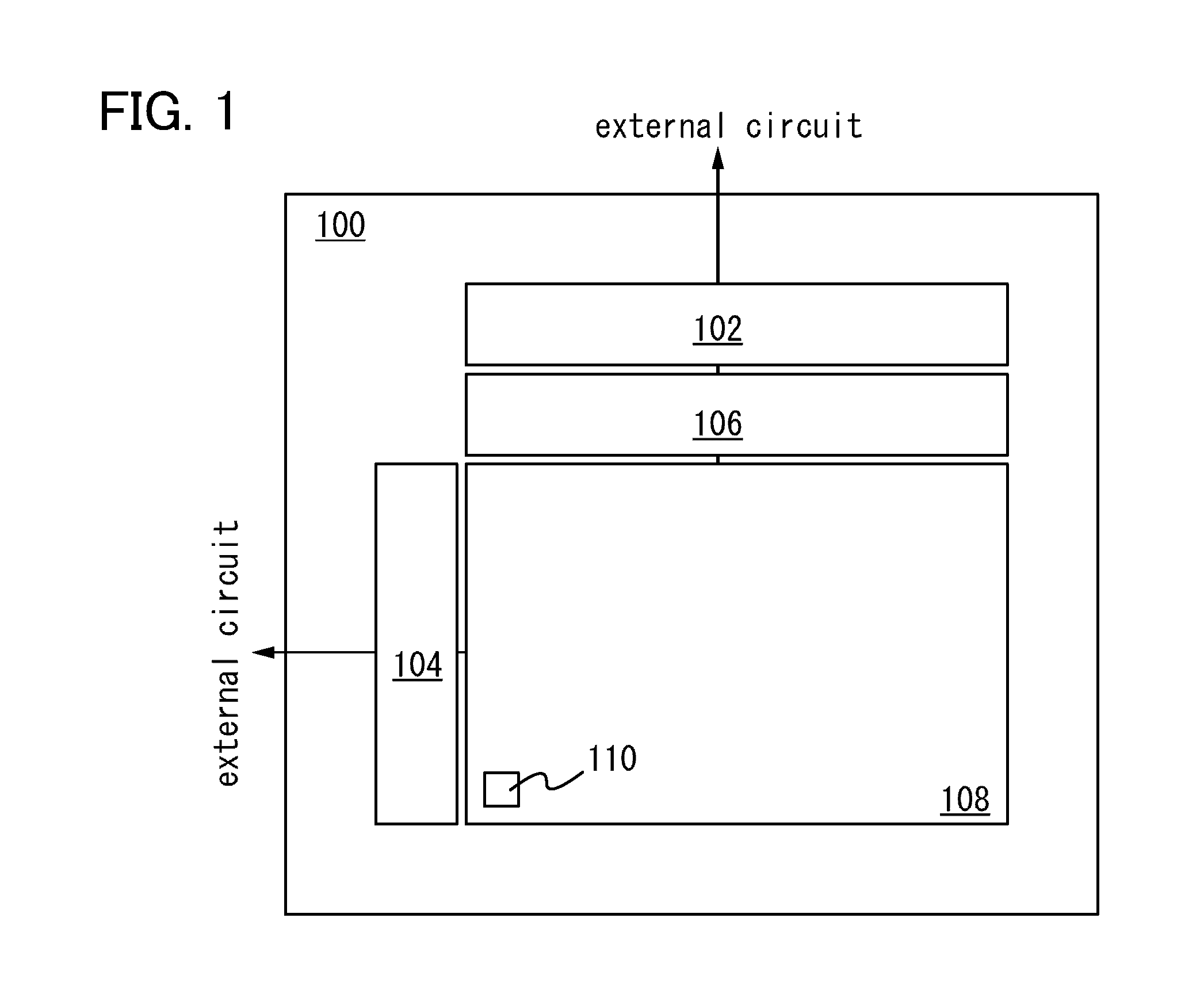
[0047]FIG. 1 illustrates an example of a configuration of an image sensor according to this embodiment. An image sensor 100 includes a first shift register 102, a second shift register 104, a reading circuit 106, and a pixel array 108. The first shift register 102 is electrically connected to the pixel array 108 through the reading circuit 106. The second shift register 104 is electrically connected to the pixel array 108. The pixel array 108 includes a plurality of pixels 110. The pixels 110 are arranged in a matrix in the pixel array 108. Data which is output from the pixel array 108 is output to an external circuit of the image sensor 100 through the reading circuit 106.

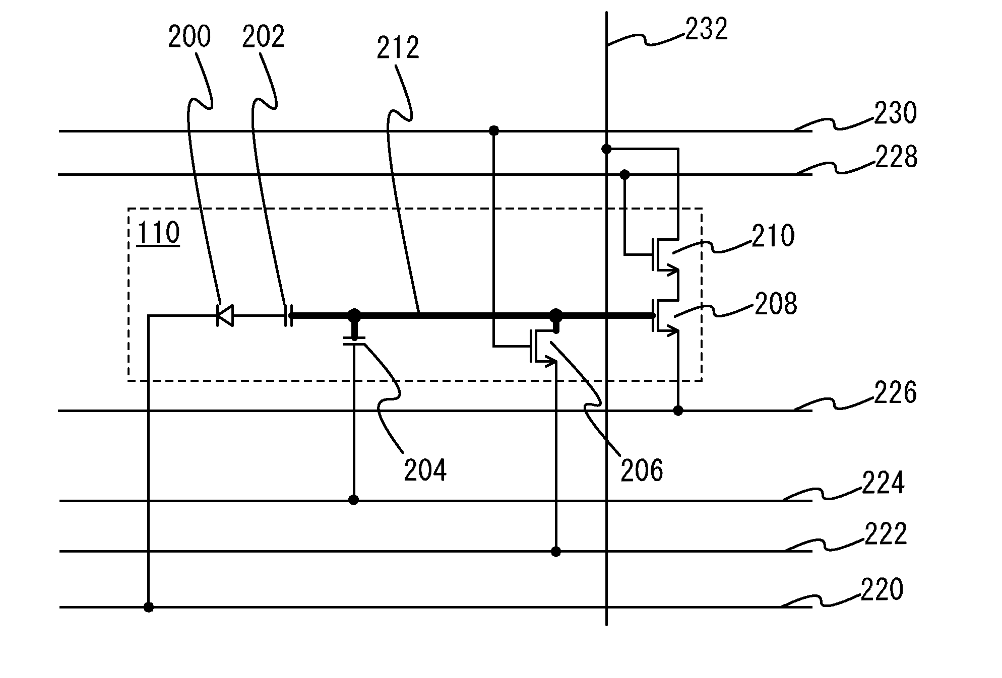
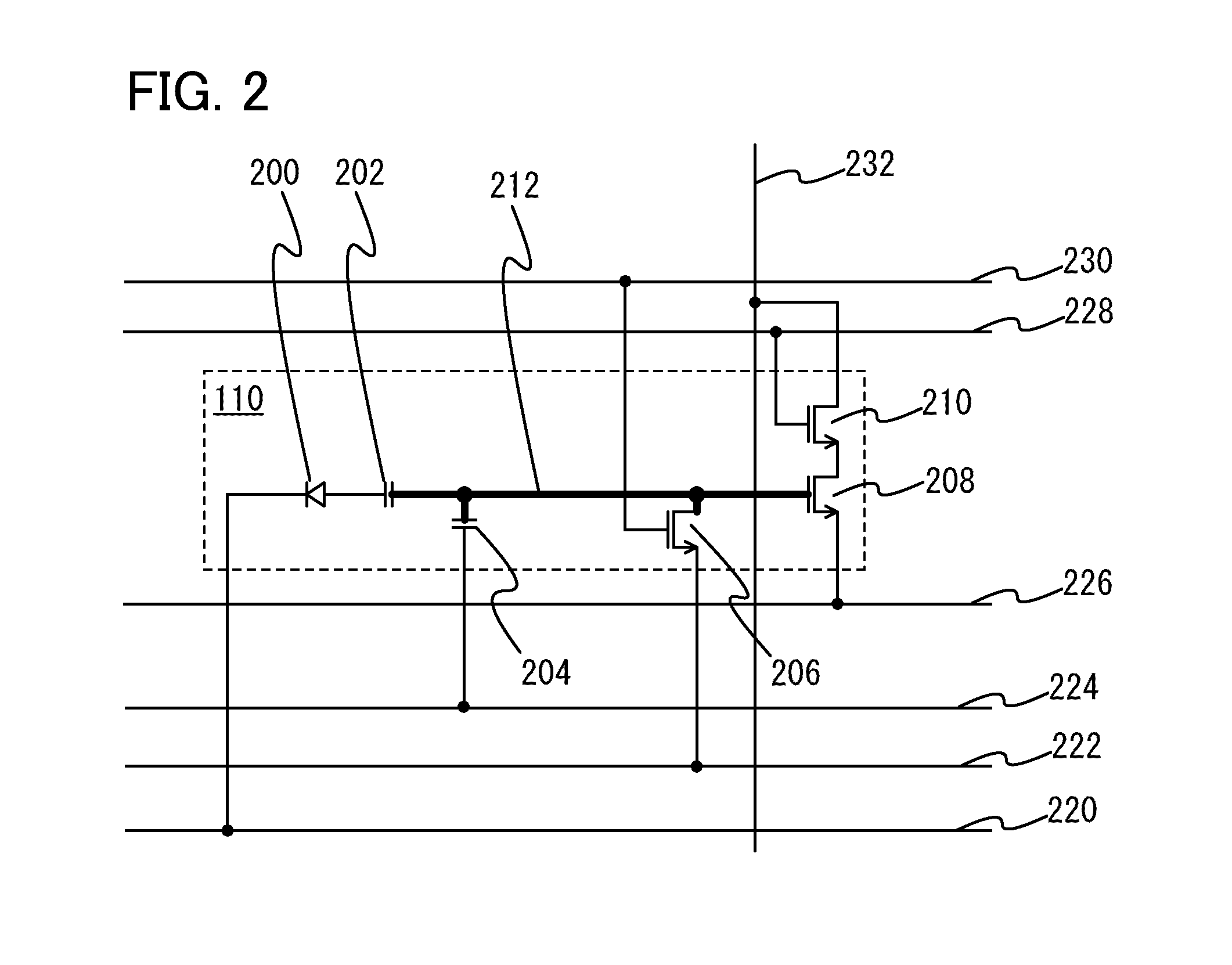
[0048]FIG. 2 illustrates an example of a circuit configuration of the pixel 110. A circuit of the pixel 11...

embodiment 2

[0078]In one embodiment of the present invention, a global shutter method may be employed. In this embodiment, a circuit configuration of a global shutter image sensor which is one embodiment of the present invention will be described with reference to FIG. 4.

[0079]An image sensor illustrated in FIG. 4 has a configuration in which a fourth transistor 400 is provided between the anode of the photodiode 200 and the one electrode of the first capacitor 202 in FIG. 2.

[0080]The anode of the photodiode 200 is electrically connected to a source of the fourth transistor 400. A gate of the fourth transistor 400 is electrically connected to an eighth wiring 234. The eighth wiring 234 is electrically connected to the second shift register 104. A drain of the fourth transistor 400 is electrically connected to the one electrode of the first capacitor 202. The other connections are similar to those in FIG. 2. Note that the source and the drain of the fourth transistor 400 may be interchanged with...

embodiment 3

[0086]A transistor having a channel formed in an oxide semiconductor layer is preferably used as the first transistor 206 in Embodiment 1 and Embodiment 2.

[0087]Note that in the present invention, the transistors other than the first transistor 206 are not limited to those having specific structures and may have various structures. Thus, the transistors may be formed using polycrystalline silicon or may be formed using a silicon-on-insulator (SOI) substrate. Alternatively, the transistors may be formed using a compound semiconductor substrate such as a GaAs substrate.

[0088]Although the transistors in the above description are n-channel transistors, the present invention is not limited thereto and p-channel transistors may be used as appropriate.

[0089]Next, a transistor with small off-state current which can be used in the present invention will be described. As an example of the transistor with small off-state current, there is a transistor containing a metal oxide which has semicon...


PUM


Abstract

An image sensor is provided which is capable of holding data for one frame period or longer and conducting a difference operation with a small number of elements. A photosensor is provided in each of a plurality of pixels arranged in a matrix, each pixel accumulates electric charge in a data holding portion for one frame period or longer, and an output of the photosensor changes in accordance with the electric charge accumulated in the data holding portion. As a writing switch element for the data holding portion, a transistor with small leakage current (sufficiently smaller than 1×10⁻¹⁴ A) is used. As an example of the transistor with small leakage current, there is a transistor having a channel formed in an oxide semiconductor layer.

Description

BACKGROUND OF THE INVENTION[0001]1. Field of the Invention[0002]The present invention relates to a semiconductor device and a method for driving the semiconductor device. Specifically, the present invention relates to an image sensor provided with a photosensor in each of a plurality of pixels, and a method for driving the image sensor. The present invention further relates to an electronic device including the image sensor.[0003]Note that a semiconductor device refers to a semiconductor element itself or a device including a semiconductor element. As an example of such a semiconductor element, for example, a thin film transistor can be given. Therefore, the semiconductor device includes a liquid crystal display device, a memory device, and the like.[0004]A photosensor refers to one element provided in a pixel, and an image sensor refers to a device including a plurality of pixels each provided with a photosensor.[0005]2. Description of the Related Art[0006]Image sensors are widely ...

Claims


Application Information

Patent Timeline
Patent Type & Authority Patents(United States)
IPC IPC(8): G09G3/36H01L27/146
CPCH01L27/14601H01L27/14614H01L29/22H01L27/14643H01L29/24H01L29/7869H01L27/14605H01L27/14636H01L27/14612H04N25/70
Inventor IKEDA, TAKAYUKI
Owner SEMICON ENERGY LAB CO LTD
Why Eureka
Try Eureka