Multi-chip module with stacked face-down connected dies

a technology of face-down connection and chip module, which is applied in the manufacture of printed circuits, printed circuit aspects, basic electric elements, etc., can solve the problem that the approach offers only limited reduction in the aggregate area of the circuit panel occupied

Active Publication Date: 2014-09-23
TESSERA INC
View PDF24 Cites 57 Cited by
  • Summary
  • Abstract
  • Description
  • Claims
  • Application Information

AI Technical Summary

Problems solved by technology

This approach offers only limited reduction in the aggregate area of the circuit panel occupied by the chips.

Method used


Image

  • Multi-chip module with stacked face-down connected dies
  • Multi-chip module with stacked face-down connected dies
  • Multi-chip module with stacked face-down connected dies

Examples


Embodiment Construction

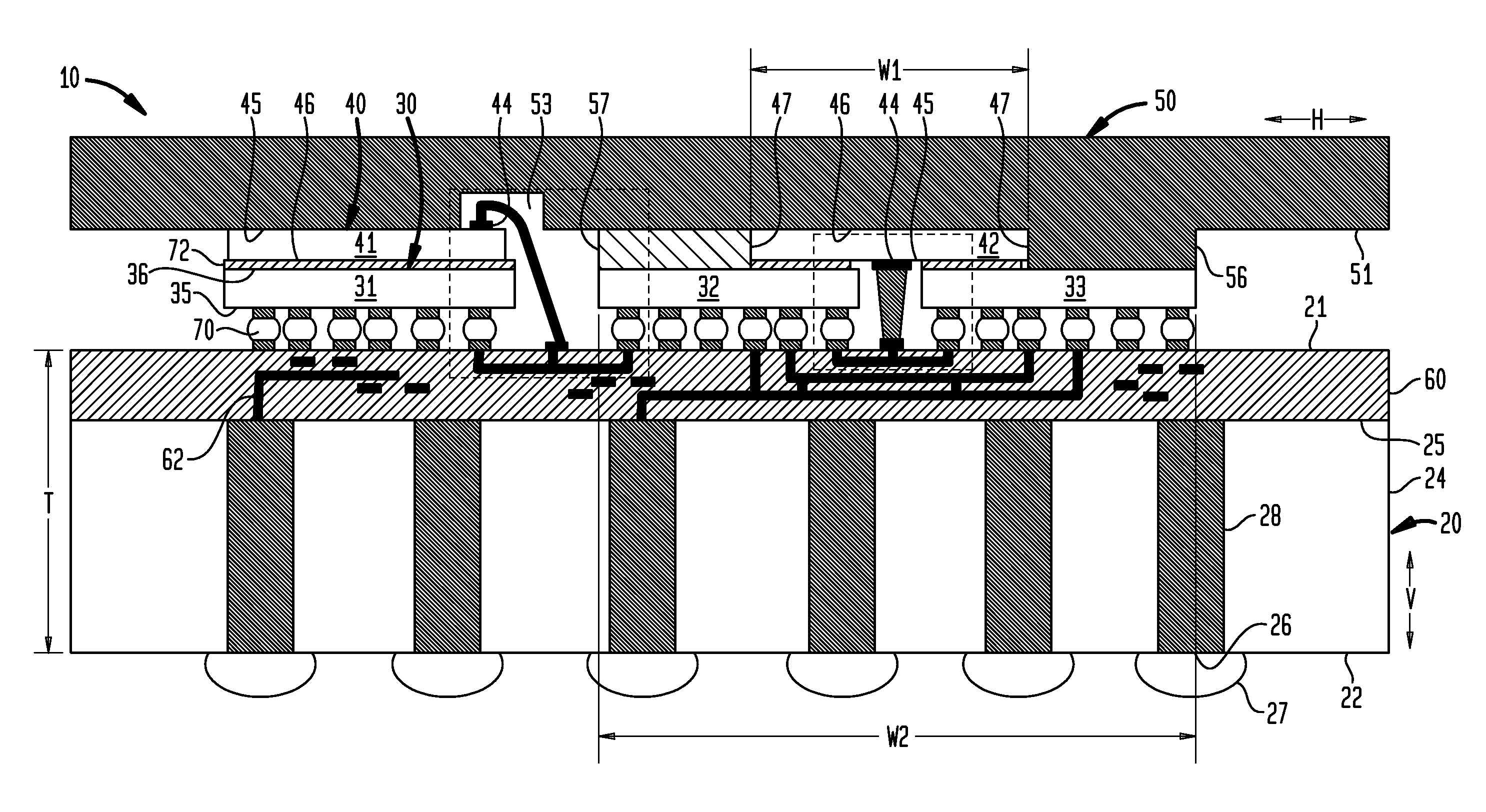
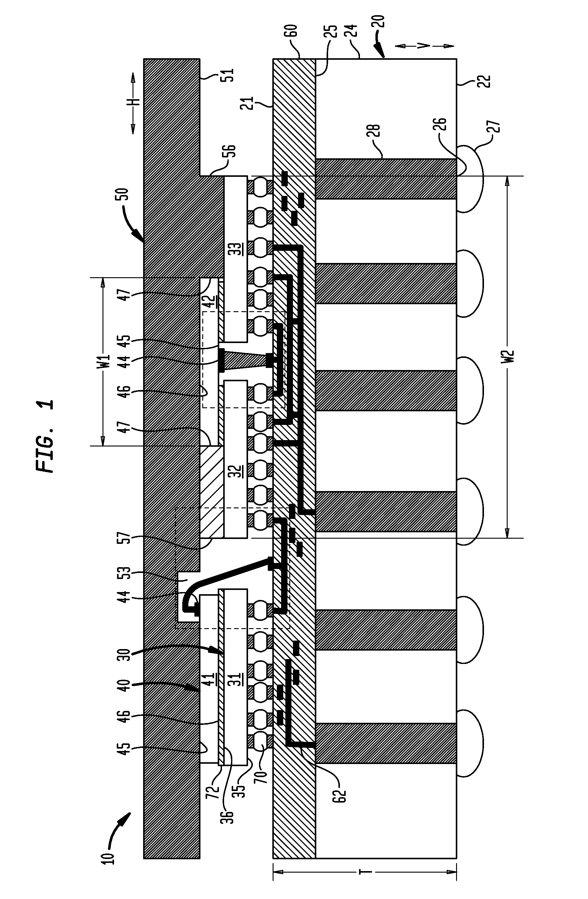
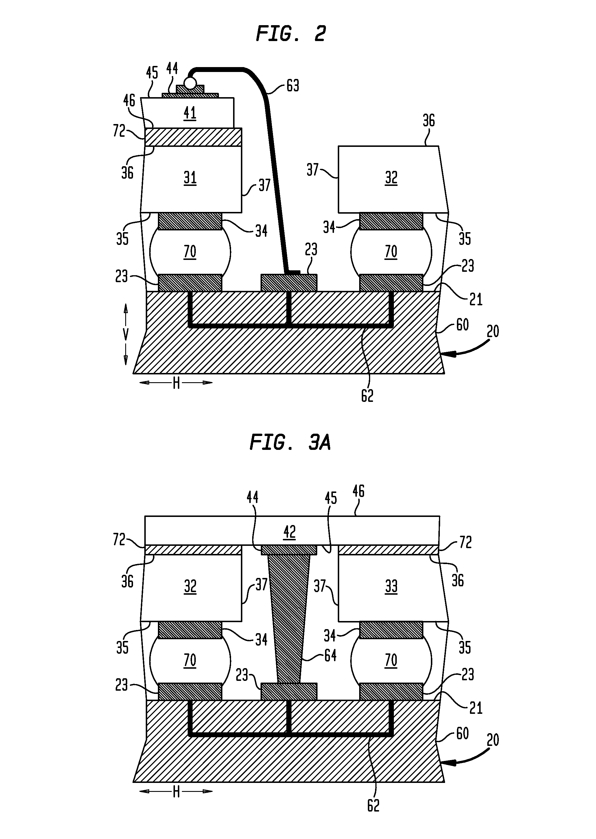
[0035]With reference to FIG. 1, a microelectronic assembly according to an embodiment of the present invention includes an interconnection substrate 20, logic chips 30 overlying a first surface 21 of the substrate 20, memory chips 40, each memory chip at least partially overlying a rear surface 36 of at least one of the logic chips, and at least one heat spreader 50 overlying a surface of each memory chip.

[0036]In FIG. 1, the directions parallel to the first surface 21 are referred to herein as “horizontal” or “lateral” directions, whereas the directions perpendicular to the front surface are referred to herein as upward or downward directions and are also referred to herein as the “vertical” directions. The directions referred to herein are in the frame of reference of the structures referred to. Thus, these directions may lie at any orientation to the normal or gravitational frame of reference. A statement that one feature is disposed at a greater height “above a surface” than ano...


PUM


Abstract

A microelectronic assembly can include a substrate having first and second surfaces, at least two logic chips overlying the first surface, and a memory chip having a front surface with contacts thereon, the front surface of the memory chip confronting a rear surface of each logic chip. The substrate can have conductive structure thereon and terminals exposed at the second surface for connection with a component. Signal contacts of each logic chip can be directly electrically connected to signal contacts of the other logic chips through the conductive structure of the substrate for transfer of signals between the logic chips. The logic chips can be adapted to simultaneously execute a set of instructions of a given thread of a process. The contacts of the memory chip can be directly electrically connected to the signal contacts of at least one of the logic chips through the conductive structure of the substrate.

Description

BACKGROUND OF THE INVENTION[0001]The present invention relates to stacked microelectronic assemblies and methods of making such assemblies, and to components useful in such assemblies.[0002]Semiconductor chips are commonly provided as individual, prepackaged units. A standard chip has a flat, rectangular body with a large front face having contacts connected to the internal circuitry of the chip. Each individual chip typically is mounted in a package which, in turn, is mounted on a circuit panel such as a printed circuit board and which connects the contacts of the chip to conductors of the circuit panel. In many conventional designs, the chip package occupies an area of the circuit panel considerably larger than the area of the chip itself.[0003]As used in this disclosure with reference to a flat chip having a front face, the “area of the chip” should be understood as referring to the area of the front face. In “flip chip” designs, the front face of the chip confronts the face of a...

Claims


Application Information

Patent Timeline
Patent Type & Authority Patents(United States)
IPC IPC(8): H01L23/34
CPCH01L23/13H01L25/0652H01L23/49827H01L2224/73253H01L2224/48227H01L24/32H01L2924/15311H01L23/367H01L2924/15192H01L2224/33181H01L25/50H05K2201/10159H01L25/18H01L2225/06558H01L2924/07811H05K3/303H01L24/16H01L2924/01322H01L24/48H01L2224/73265H01L2224/48465H01L2224/16227H01L2224/13147H01L2224/73215H01L2924/01029H01L2224/16225H01L2224/131H01L2924/09701H01L2224/32145H01L24/73H01L25/0657H01L2224/0401H01L2224/04042H01L2224/16235H01L2224/32245H01L2224/48235H01L2224/73203H01L2225/0651H01L2225/06517H01L2225/06589H01L2924/1431H01L2924/1434H01L2924/15159H01L2924/18161H01L2924/15174H01L2924/15184H01L2924/00014H01L2924/00012H01L2924/014H01L2924/00H01L2224/45099H01L2224/45015H01L2924/207H01L23/12H01L25/065H01L23/02H01L23/3675H01L23/5386H01L24/17H01L24/49H01L2224/48106H01L2224/73257H01L2924/20645
Inventor HABA, BELGACEMMOHAMMED, ILYASSAVALIA, PIYUSH
Owner TESSERA INC
Why Eureka
Try Eureka