Mask blank, transfer mask and process for manufacturing semiconductor devices
a technology of transfer mask and semiconductor device, which is applied in the field of mask blank and transfer mask, can solve the problems of insufficient production of mask blanks with high flatness, poor flatness of glass substrate immediately after being cut out, and poor surface condition of main surfaces, so as to suppress tantalum oxidation, reduce light shielding performance, and reduce the effect of tantalum oxidation
- Summary
- Abstract
- Description
- Claims
- Application Information
AI Technical Summary
Benefits of technology
Problems solved by technology
Method used
Image

Examples
example 1
Production of Mask Blank of Example 1
[0112]A synthetic quartz ingot produced by a conventional production method (a soot method) was heat treated at not less than 1000° C. for at least 2 hours. Next, the heat treated synthetic quartz ingot was cut to give a synthetic quartz glass substrate having a length and width sizes of about 152 mm×152 mm and a thickness of 6.85 mm. Chamfer faces were appropriately formed.
[0113]The cut-out glass substrate was subjected to grinding on the main surfaces and end faces (side faces and chamfer faces). The main surfaces of the ground glass substrate were sequentially subjected to a rough polishing step and a precision polishing step. In detail, the glass substrate supported by a carrier was sandwiched between upper and lower surface plates of a double surface polishing device whose respective surfaces were fitted with polishing pads (hard polishers), and was caused to undergo a planetary gear motion while supplying a polishing liquid containing ceriu...
example 2
Production of Mask Blank of Example 2
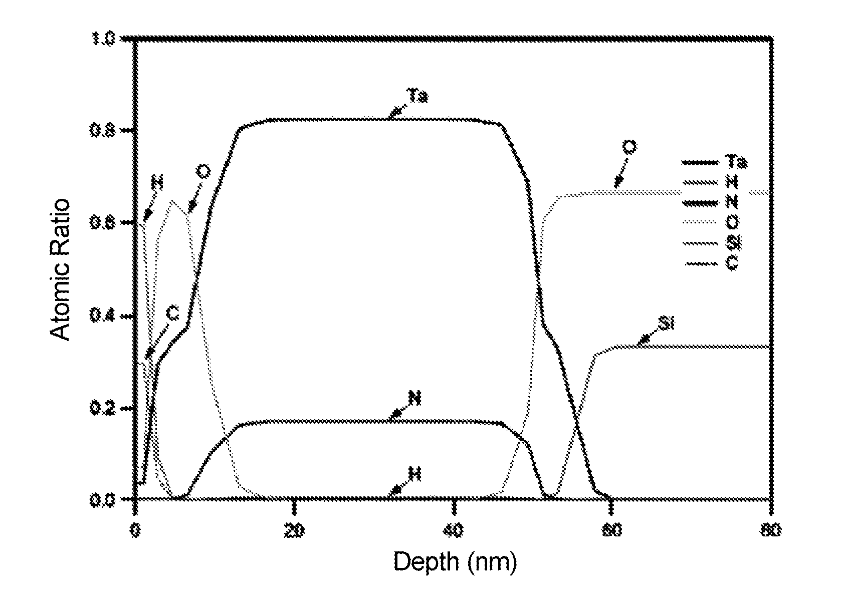
[0135]A glass substrate of synthetic quartz which was similar to that used in Example 1 was polished and washed in the same manner, thereby preparing a washed glass substrate 1. Next, the washed glass substrate 1 was introduced into a DC magnetron sputtering device equipped with a Si (silicon) target. A mixed gas containing Ar and NO was supplied into the sputtering device, and the Si target was sputtered to form a invasion suppressive film (a SiON layer) 6 with a film thickness of 30 nm in contact with the main surface of the glass substrate 1. Next, the glass substrate 1 with the invasion suppressive film 6 was introduced into a sputtering device equipped with a tantalum target. Similarly to Example 1, a mixed gas containing Xe and N2 was supplied and the tantalum target was sputtered to form a TaN layer (a lower layer) 2 with a film thickness of 43 nm on the surface of the invasion suppressive film 6. Next, the gas in the sputtering device was...
PUM
| Property | Measurement | Unit |
|---|---|---|
| thickness | aaaaa | aaaaa |
| thickness | aaaaa | aaaaa |
| binding energy | aaaaa | aaaaa |
Abstract
Description
Claims
Application Information