Wafer cutting method and a system thereof

a cutting method and a technology of a cutting system, applied in the direction of laser beam welding apparatus, welding/soldering/cutting articles, electrical equipment, etc., can solve the problems of cracking and cracking of the wafer

Active Publication Date: 2014-09-30
AGENCY FOR SCI TECH & RES
View PDF11 Cites 1 Cited by
  • Summary
  • Abstract
  • Description
  • Claims
  • Application Information

AI Technical Summary

Benefits of technology

[0013]In a first aspect of the present invention, there is provided a method for cutting a semiconductor wafer by generating a crack within the wafer. The method comprises irradiating a laser beam towards a surface of the wafer and converging the laser beam to form a focal point so that a focal volume defined by the focal point and a boundary of the laser beam within the wafer is formed. Energy encompassed within the focal volume causes the wafer located at the periphery of the focal volume to contract faster than the wafer located within the focal volume, thereby generating a crack within the wafer. Preferably, the irradiating comprises irradiating a laser beam having a laser power density lower than the vapourisation threshold of the wafer ablation.
[0014]In a second aspect of the present invention, there is provided a system for cutting a semiconductor wafer by generating a crack within the wafer. The system comprises a laser beam source for irradiating a laser beam towards a surface of the wafer and a converging lens to converge the laser beam to form a focal point so that a focal volume defined by the focal point and a boundary of the laser beam within the wafer is formed. Energy encompassed within the focal volume causes the wafer located at the periphery of the focal volume to contract faster than the wafer located within the focal volume, thereby generating a crack within the wafer.

Problems solved by technology

Energy encompassed within the focal volume causes the wafer located at the periphery of the focal volume to contract faster than the wafer located within the focal volume, thereby generating a crack within the wafer.

Method used


Image

  • Wafer cutting method and a system thereof
  • Wafer cutting method and a system thereof
  • Wafer cutting method and a system thereof

Examples


first embodiment

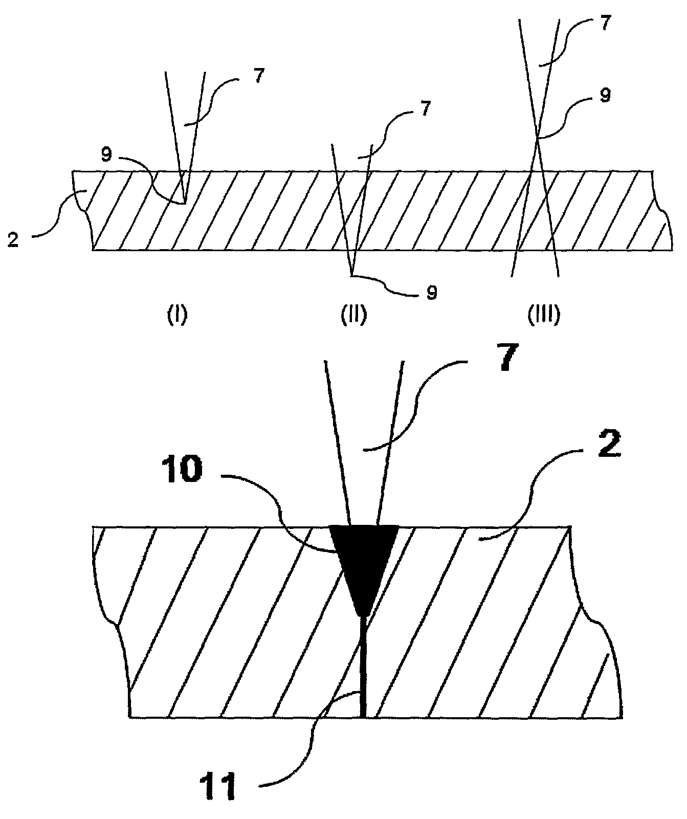
[0024]In accordance with the invention illustrated in FIG. 1, there is provided a platform table 1 for holding and moving a silicon wafer 2 to be cut into individual silicon chips. The platform table 1 is capable of moving in the x-y axis via manipulation of a control device 8, such as a computer.

[0025]A laser beam source 4 is provided to irradiate a laser beam 7 onto a surface of the wafer 2 held on the platform table 1. The laser beam source 4 includes, but is not limited to, excimer laser, Nd:YAG laser, CO2 laser, fiber laser, and any other near infrared laser. Preferably, the laser beam source 4 is a fiber laser.

[0026]Optionally, a laser beam guide 6 is provided to guide the laser beam 7 irradiated from the laser beam source 4 towards the surface of the wafer 2, the laser beam 7 passing through a focusing lens 3. The laser beam guide 6 may be a flat reflecting mirror, positioned at an angle to reflect the direction of the laser beam 7.

[0027]The focusing lens 3 is provided to con...

second embodiment

[0035]In accordance with the invention illustrated in FIG. 5, there is provided a platform table 1 for holding and moving a silicon wafer 2 to be cut into individual silicon chips. The platform table 1 is capable of moving in the x-y axis via manipulation of a control device 8, such as a computer.

[0036]A laser beam source 4 is provided to irradiate a laser beam 7 onto a surface of the wafer 2 held on the platform table 1. The laser beam source 4 includes, but is not limited to, excimer laser, Nd:YAG laser, CO2 laser, fiber laser, and any other near infrared laser. Preferably, the laser beam source 4 is a fiber laser.

[0037]Optionally, a laser beam guide 6 is provided to guide the laser beam 7 irradiated from the laser beam source 4 towards the surface of the wafer 2, the laser beam 7 passing through a focusing lens 3 (FIG. 6). The laser beam guide 6 may be a flat reflecting mirror, positioned at an angle to reflect the direction of the laser beam 7.

[0038]The beam shaper 29 is provide...


PUM

PropertyMeasurementUnit
pulse duration timeaaaaaaaaaa
infrared wavelengthaaaaaaaaaa

Abstract

A method for cutting a semiconductor wafer by generating a crack within the wafer, and a system thereof, are provided. The method comprises irradiating a laser beam towards a surface of the wafer and converging the laser beam to form a focal point so that a focal volume defined by the focal point and a boundary of the laser beam within the wafer is formed. Energy encompassed within the focal volume causes the wafer located at the periphery of the focal volume to contract faster than the wafer located within the focal volume, thereby generating a crack within the wafer.

Description

CROSS-REFERENCE TO RELATED APPLICATION[0001]This application claims the benefits of Singapore Patent Application No. 200809032-6 filed on 5 Dec. 2008 and 200904047-8 filed on 12 Jun. 2009, the entire contents of which are incorporated herein by reference.FIELD OF INVENTION[0002]The invention relates to a method for cutting or dicing a semiconductor wafer by generating a crack within the wafer, and a system thereof. More particularly, the method relates to cutting the wafer with a laser beam.BACKGROUND TO THE INVENTION[0003]The following discussion of the background to the invention is intended to facilitate an understanding of the present invention. However, it should be appreciated that the discussion is not an acknowledgment or admission that any of the material referred to was published, known or part of the common general knowledge in any jurisdiction as at the priority date of the application.[0004]Semiconductor wafer cutting or dicing is a cutting operation that is being emplo...

Claims


Application Information

Patent Timeline
Patent Type & Authority Patents(United States)
IPC IPC(8): B23K26/00B23K26/14B23K26/02B23K26/40H01L21/78
CPCH01L21/78B23K26/4075B23K2201/40Y10T225/304B23K26/40B23K2103/50B23K2101/40
Inventor WANG, ZHONGKECHEN, TAOZHENG, HONGYU
Owner AGENCY FOR SCI TECH & RES
Why Eureka
Try Eureka