Organic light-emitting diode and method of fabricating the same

a light-emitting diode and organic technology, applied in the direction of discharge tube/lamp details, discharge tube luminescnet screens, semiconductor/solid-state device details, etc., can solve the problems of light output efficiency and color properties limitations of conventional organic light-emitting diodes, prevent the increase of fabrication costs, and improve light output efficiency and color properties

Active Publication Date: 2014-09-30
LG DISPLAY CO LTD
View PDF6 Cites 3 Cited by
  • Summary
  • Abstract
  • Description
  • Claims
  • Application Information

AI Technical Summary

Benefits of technology

[0018]An object of the present disclosure is to provide an organic light-emitting diode display device with improved light output efficiency and color properties.
[0019]Another object of the present disclosure is to provide a method of fabricating an organic light-emitting diode display device, capable of improving light output efficiency without an additional mask process for preventing a fabrication cost from increasing and a fabrication process from being complicated.

Problems solved by technology

However, the conventional organic light-emitting diode has limitations in light output efficiency and color properties.

Method used


Image

  • Organic light-emitting diode and method of fabricating the same
  • Organic light-emitting diode and method of fabricating the same
  • Organic light-emitting diode and method of fabricating the same

Examples


first embodiment

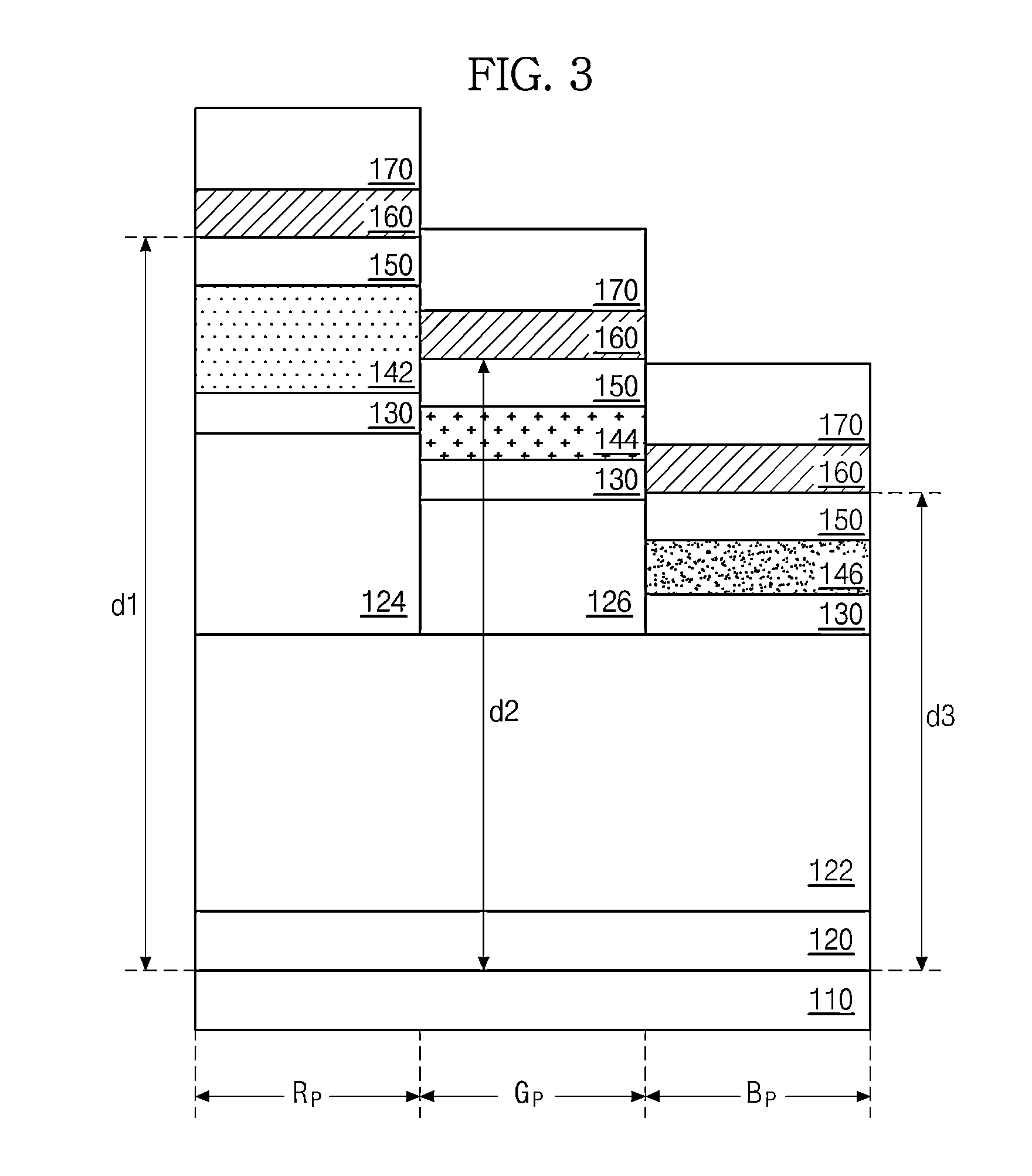
[0032]FIG. 3 is a cross-sectional view of an organic light-emitting diode according to the present invention.

[0033]As shown in FIG. 3, the organic light-emitting diode includes an anode 110 applied on a substrate (not shown) on which red, green, and blue pixel areas Rp, Gp, and Bp are defined, a hole injection layer 120, a first hole transporting layer 122, a second hole transporting layer 124, a third hole transporting layer 126, an electron blocking layer 130, an emitting material layer consisting of a red organic light-emitting pattern 142, a green organic light-emitting pattern 144, and a blue organic light-emitting pattern 146, an electron transporting layer 150, a cathode 160, and a capping layer 170.

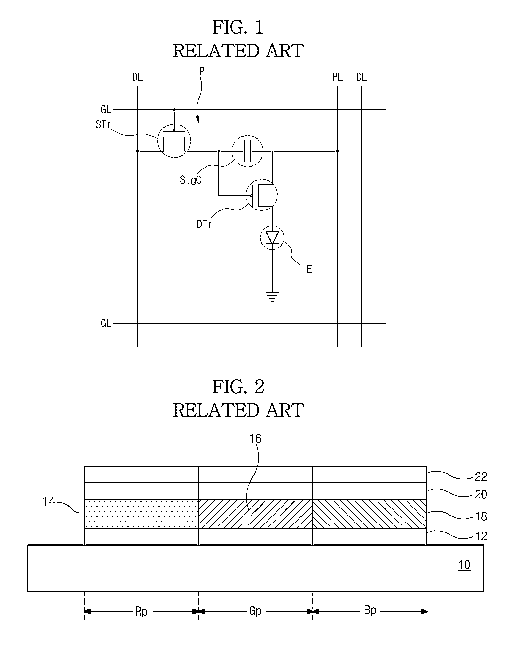
[0034]Also, although not shown in FIG. 3, in an organic light-emitting diode display device including the organic light-emitting diode, a power line is disposed to extend parallel to one of gate lines and data lines that cross each other on the substrate to define the pixel areas ...

second embodiment

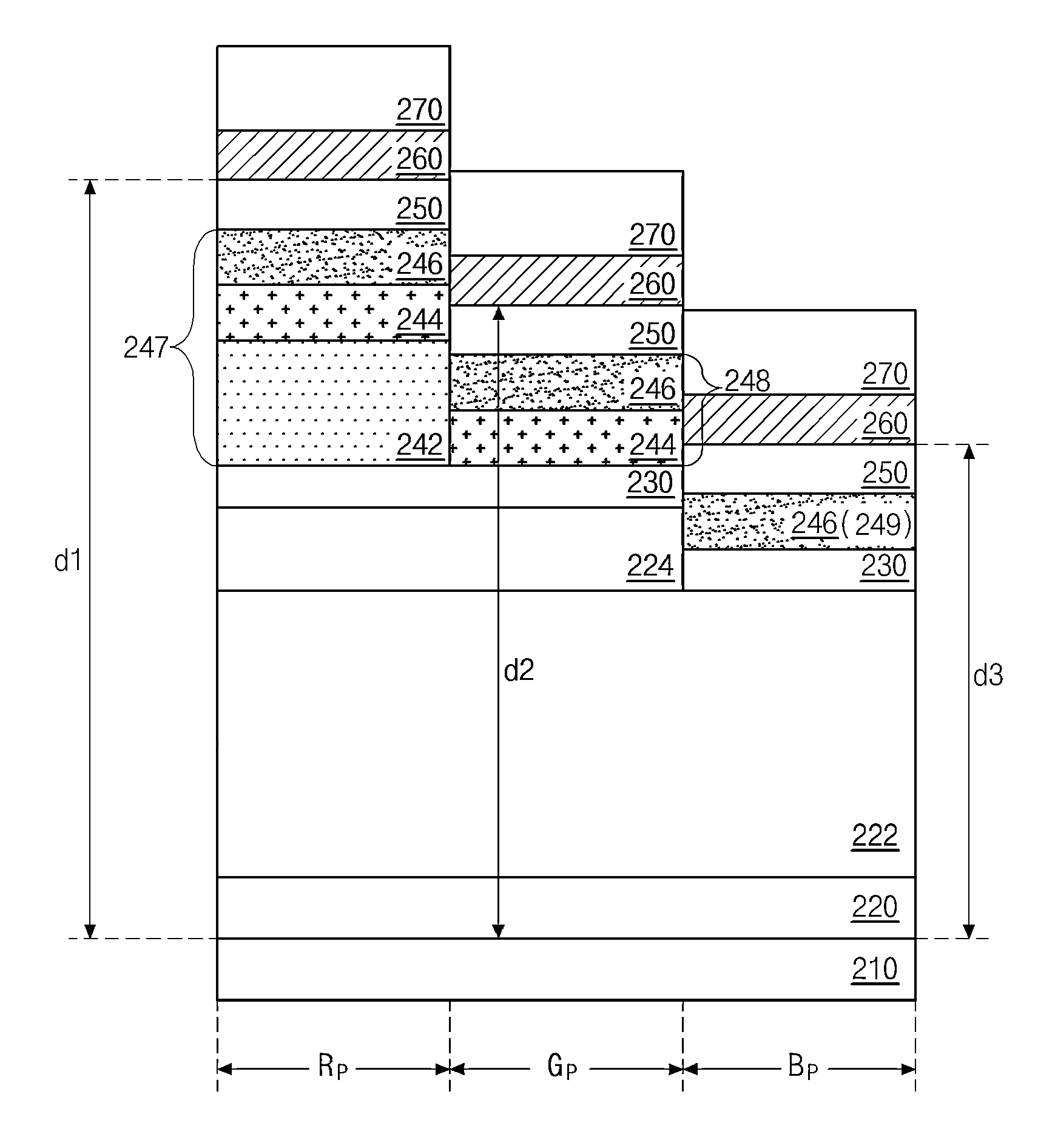
[0056]Hereinafter, an organic light-emitting diode capable of overcoming this problem will be described with reference to FIG. 4, which is a cross-sectional view of an organic light-emitting diode according to the present invention.

[0057]As shown in FIG. 4, the organic light-emitting diode includes an anode 210, a hole injection layer 220, a first hole transporting layer 222, a second hole transporting layer 224, an electron blocking layer 230, an emitting material layer consisting of a red organic light-emitting pattern 242, a green organic light-emitting pattern 244, and a blue organic light-emitting pattern 246, an electron transporting layer 250, a cathode 260, and a capping layer 270 stacked on a substrate (not shown) on which red, green, and blue pixel areas Rp, Gp, and Bp are defined.

[0058]Although not shown in FIG. 4, in an organic light-emitting diode display device including the organic light-emitting diode, a power line is disposed to extend parallel to one of gate lines ...


PUM


Abstract

An organic light-emitting diode includes an anode on a substrate; a first hole transporting layer on the anode; a second hole transporting layer on the first hole transporting layer and corresponding to the red and green pixel areas; a first emitting material pattern of a first thickness on the second hole transporting layer and corresponding to the red pixel area; a second emitting material pattern of a second thickness on the second hole transporting layer and corresponding to the green pixel area; a third emitting material pattern of a third thickness on the first hole transporting layer and corresponding to the blue pixel area; an electron transporting layer on the first, second and third emitting material patterns; and a cathode on the electron transporting layer, wherein the second thickness is less than the first thickness and greater than the third thickness.

Description

[0001]The present application claims the priority benefit of Korean Patent Application No. 10-2012-0092979 filed in Republic of Korea on Aug. 24, 2012, which is hereby incorporated by reference.BACKGROUND[0002]1. Field of the Disclosure[0003]The present disclosure relates to an organic light-emitting diode, and more particularly, to an organic light-emitting diode capable of reducing the number of masks required in a fabrication process to thereby reduce a fabricating cost and simplify the fabrication process, and a method of fabricating the organic light-emitting diode.[0004]2. Discussion of the Related Art[0005]A cathode ray tube (CRT) has been used as a display for various electronics for a long time. However, recently, flat panel display devices, such as a plasma display panel (PDP), a liquid crystal display (LCD), and an organic light-emitting diode (OLED) display device, have been developed and widely used.[0006]Among the above-mentioned flat panel display devices, the organic...

Claims


Application Information

Patent Timeline
Patent Type & Authority Patents(United States)
IPC IPC(8): H01L51/50
CPCH01L51/504H01L51/5064Y02E10/549H10K59/35H10K50/156H10K50/852H10K2102/351H10K71/00H01L21/02579H10K59/38H10K77/10H10K50/12H10K50/15H10K50/16H10K50/13H01L27/153
Inventor PARK, JIN-HOKIM, KWANG-HYUNKIM, MIN-NA
Owner LG DISPLAY CO LTD
Why Eureka
Try Eureka