Laser light source

a laser light source and laser technology, applied in semiconductor lasers, lighting and heating apparatus, instruments, etc., can solve the problems of restricted focusability and collimatability, certain loss of imaging properties, and disturbances in the vertical far field, so as to reduce or even prevent auxiliary emission, the effect of great suppression

Active Publication Date: 2014-10-14
OSRAM OPTO SEMICONDUCTORS GMBH & CO OHG
View PDF27 Cites 6 Cited by
  • Summary
  • Abstract
  • Description
  • Claims
  • Application Information

AI Technical Summary

Benefits of technology

[0012]Suppression of the coherent electromagnetic radiation emitted from the auxiliary emission region of the radiation coupling-out area can mean, in particular, that the disturbances brought about by the auxiliary emission in the vertical far-field beam profile, for example in the form of one or more auxiliary peaks with respect to the main peak of the main emission, are avoided or eliminated. Consequently, it is advantageously possible to utilize laser light sources comprising a semiconductor layer sequence which indeed possibly have an auxiliary emission in addition to the main emission, but in which the auxiliary emission is suppressed by the filter element in such a way that for projection imagings, for example, the desired beam properties, in particular the desired vertical far-field beam profile, are achieved.
[0044]Furthermore, the at least one cutout can be at least partly filled with a material that absorbs the coherent electromagnetic radiation and / or a thermally conductive material. It is thereby possible to achieve a better suppression of the coherent electromagnetic radiation emitted from the auxiliary emission region and / or an improved thermal linking to a heat sink, for example. Suitable materials for the absorbent material and / or the thermally conductive material include the materials mentioned above in connection with the first and second absorbers.

Problems solved by technology

Deviations of the far-field beam profile from the Gaussian beam profile lead to restricted focusability and collimatability.
Conventional production of laser diodes typically yields a proportion of diodes which, although they fulfill all performance criteria, nevertheless exhibit disturbances in the vertical far-field.
Although less highly pronounced disturbances of the vertical far-field beam profile do not necessarily lead to the rejection of the laser diodes, they may nevertheless lead to certain losses in the imaging properties.
Besides the already mentioned device selection from a 100% measurement of the far-field, which, although used successfully, at the same time increases the production costs as a result of the decrease in yield caused by rejection, or the acceptance of disturbances in the far-field which lead to losses in the projection imaging, lateral chip structures for far-field improvement are also known, thus for instance from U.S. Pat. No. 7,103,082 B2, but they cannot be applied to the vertical far-field.
However, they are very complex in terms of alignment and cannot be used for improving the vertical far-field beam profile of semiconductor lasers such as, for instance, nitride-based diode lasers.

Method used


Image

  • Laser light source
  • Laser light source
  • Laser light source

Examples


Embodiment Construction

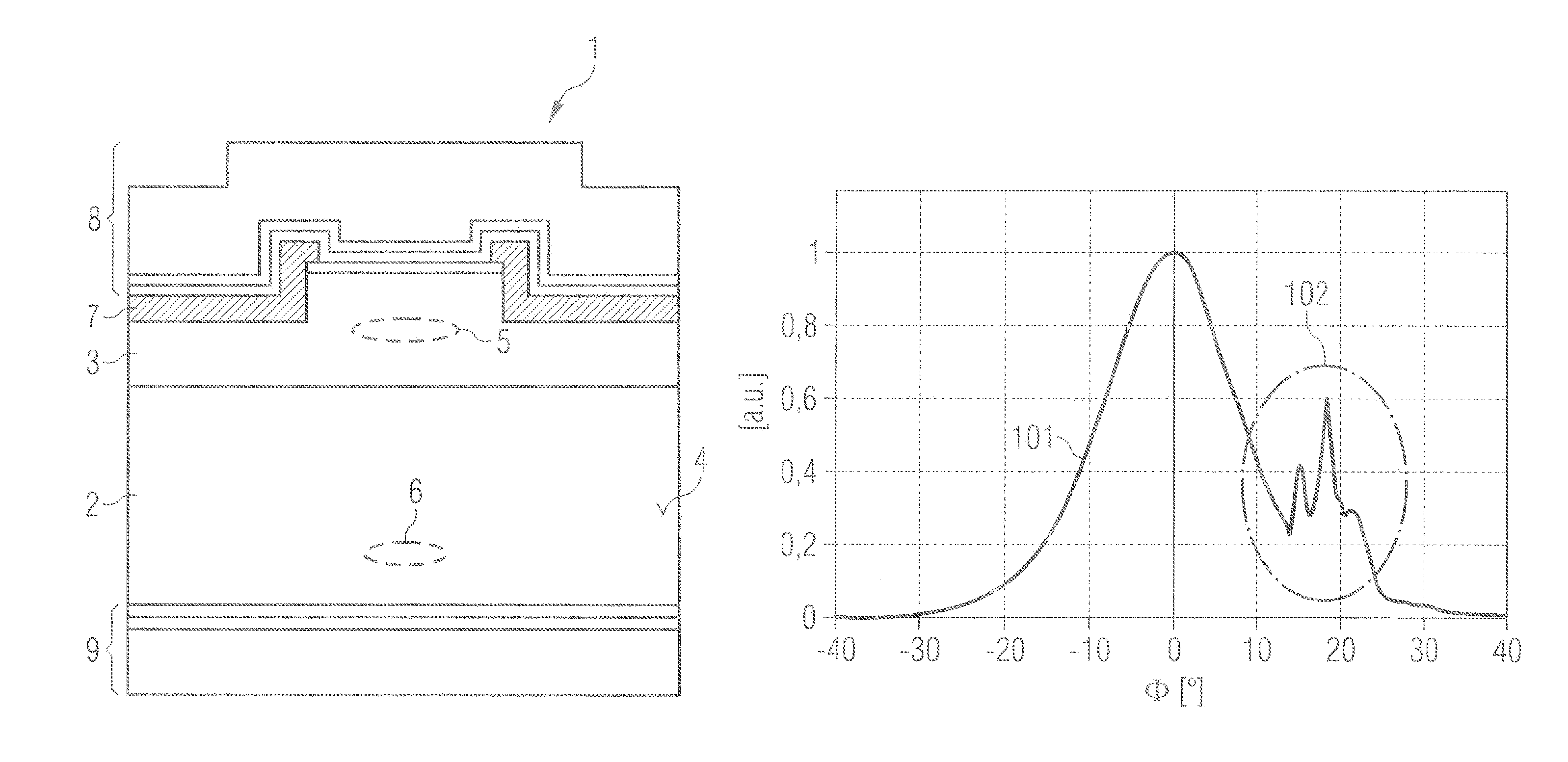
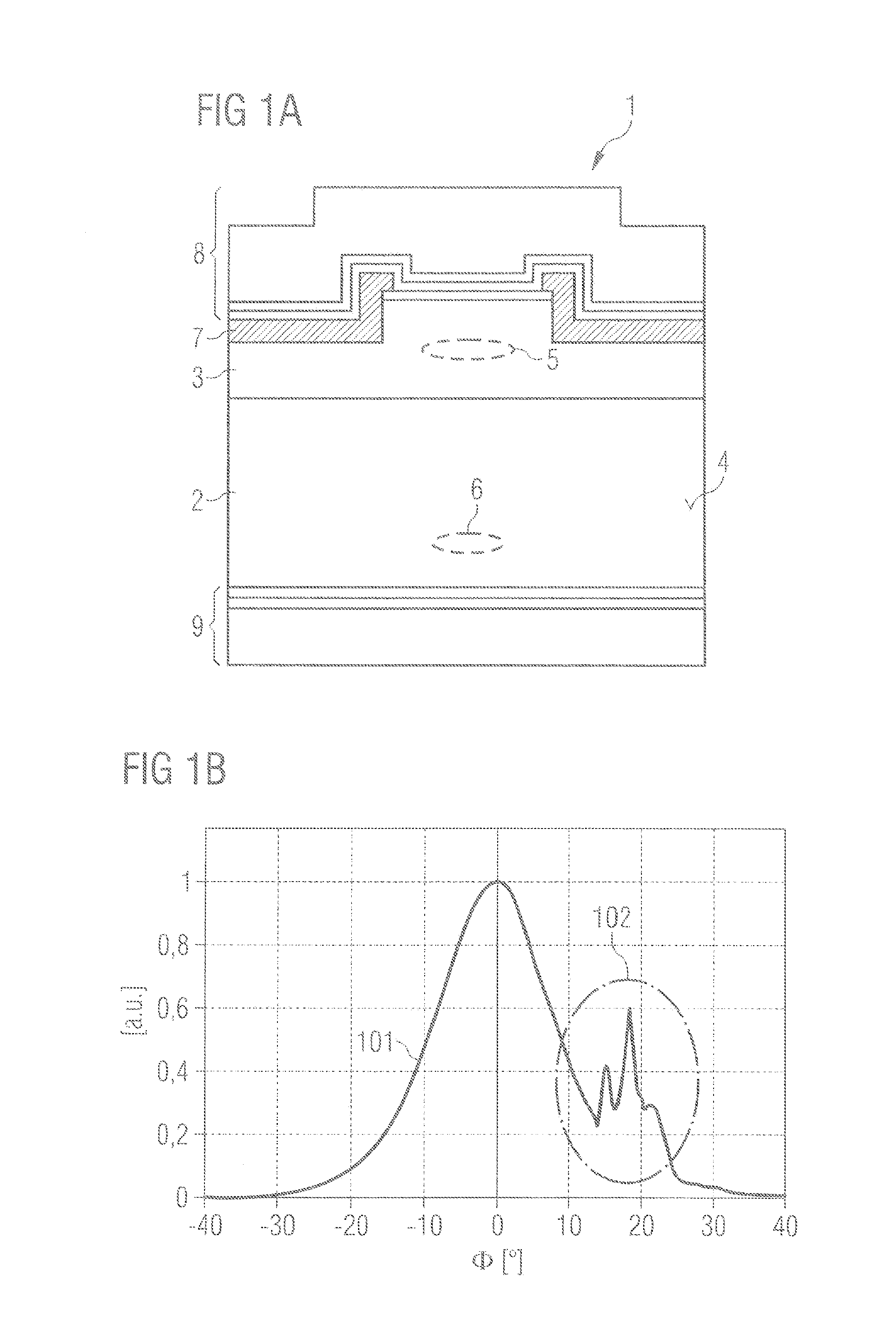
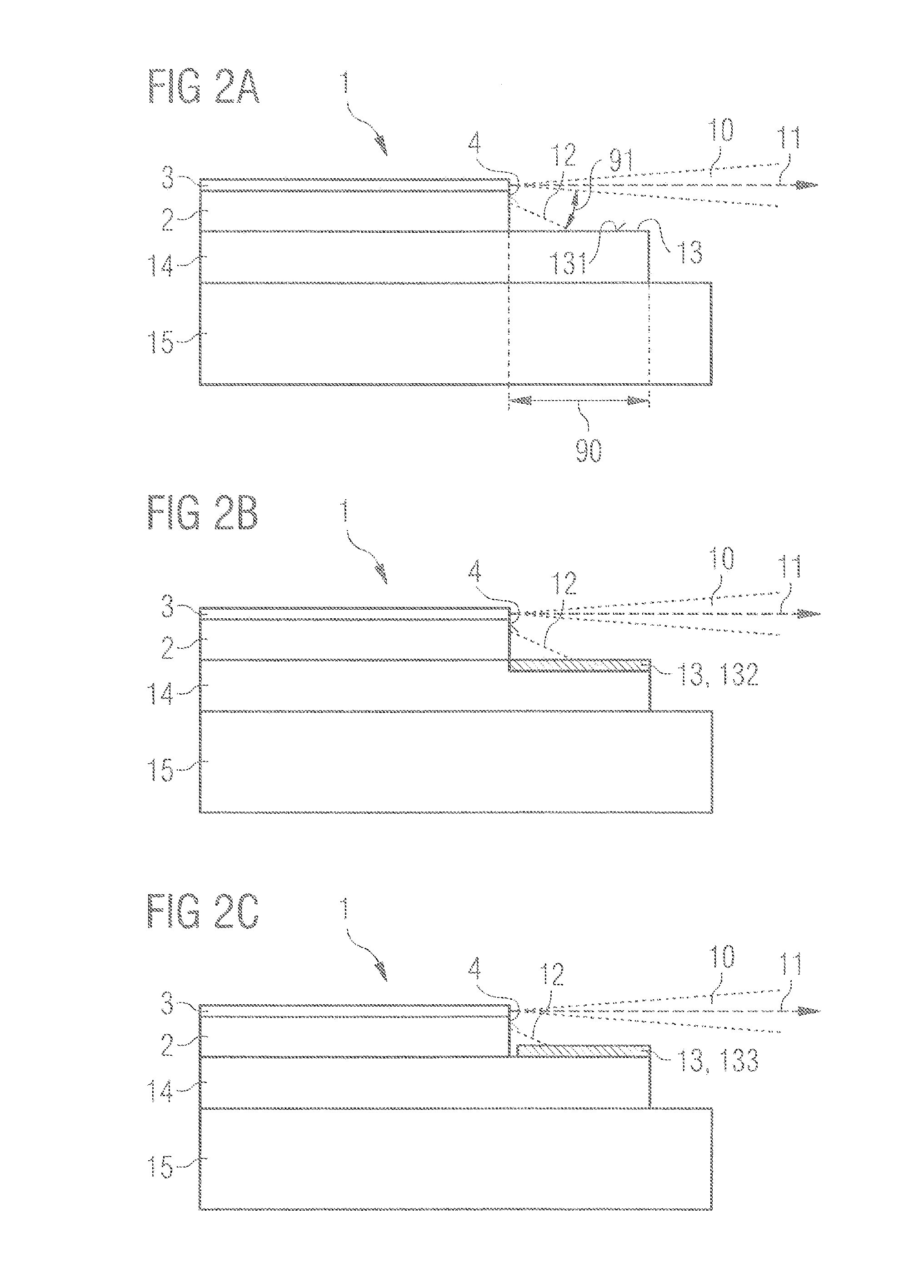
[0051]In the exemplary embodiments and figures, identical or identically acting constituent parts may in each case be provided with the same reference signs. The elements illustrated and their size relationships among one another should not be regarded as true to scale, in principle; rather, individual elements, e.g., layers, devices, components and regions, may be illustrated with exaggerated thickness or size dimensions in order to enable better illustration and / or in order to afford a better understanding.

[0052]FIG. 1 shows a semiconductor layer sequence 1 for generating coherent electromagnetic radiation. Purely by way of example, a semiconductor layer sequence 1 based on a nitride semiconductor composite system is shown in this case. As an alternative thereto, the semiconductor layer sequence can also comprise or consist of other material systems described in the general part.

[0053]The semiconductor layer sequence 1 comprises an approximately 110 μm thick n-doped GaN substrate ...


PUM


Abstract

A laser light source for emitting coherent electromagnetic radiation has a vertical far-field radiation profile, having a series of semiconductor layers for generating the coherent electromagnetic radiation. An active region is located on a substrate. The coherent electromagnetic radiation is emitted during operation in an emission direction at least from a main emission region of a radiation output surface, and the radiation output surface is formed by a side surface of the sequence of semiconductor layers. A filter element suppresses coherent electromagnetic radiation in the vertical far-field radiation profile. The radiation was generated during operation and emitted by an auxiliary emission region of the radiation output surface. The auxiliary emission region is vertically offset from and spatially separated from the main emission region.

Description

[0001]This patent application is a national phase filing under section 371 of PCT / EP2011 / 055320, filed Apr. 6, 2011, which claims the priority of German patent application 10 2010 015 197.1, filed Apr. 16, 2010, each of which is incorporated herein by reference in its entirety.TECHNICAL FIELD[0002]A laser light source is specified.BACKGROUND[0003]In many areas of application, heightened requirements are made of the beam quality of a laser diode. One example of such areas of application with heightened requirements is projection applications, for example. Since, in such applications, a laser beam is usually radiated onto a viewing screen that is sometimes far away, the quality of the far-field of the laser beam determines the quality of the projection application and thus of the image as perceived by a viewer. In this case, the quality of the far-field beam profile governs, in particular, the focusability and collimatability of the laser beam, for which reason monomode laser diodes h...

Claims


Application Information

Patent Timeline
Patent Type & Authority Patents(United States)
IPC IPC(8): F21V9/00H01S5/00H01S5/022H01S5/024H01S5/026H01S5/028H01S5/0683H01S5/10H01S5/20H01S5/22
CPCH01S5/0078H01S5/0286H01S5/02461H01S5/0264H01S5/02476H01S5/2022H01S5/1085H01S5/0683H01S5/02252H01S2301/18H01S5/22H01S5/02212H01S5/02326H01S5/024H01S5/028H01S5/10
Inventor AVRAMESCU, ADRIANLELL, ALFREDTAUTZ, SOENKEBREIDENASSEL, ANDREAS
Owner OSRAM OPTO SEMICONDUCTORS GMBH & CO OHG
Why Eureka
Try Eureka