Semiconductor device having output circuit and operating method thereof

a technology of output circuit and semiconductor device, which is applied in the direction of pulse manipulation, pulse technique, instruments, etc., can solve the problems of difficult to secure the integrity of output signal, low output signal reliability, so as to achieve significant improvement in output signal reliability

Active Publication Date: 2014-10-21
SK HYNIX INC
View PDF6 Cites 0 Cited by
  • Summary
  • Abstract
  • Description
  • Claims
  • Application Information

AI Technical Summary

Benefits of technology

[0022]Various embodiments of the present invention are directed to a data output circuit of a low-power semiconductor device that may secure signal integrity of data signal without being assisted by termination control circuit.
[0026]In accordance with the embodiments of the present invention, a slew rate may be controlled based on the driving force of an output signal even in a low-power semiconductor device without a separate termination control circuit such as an ODT circuit, whereby it may be possible to secure a data eye. That is to say, the reliability of an output signal may be significantly improved.

Problems solved by technology

In general, in a low-power semiconductor device (i.e., designed to operate under low power condition), an output circuit is desirable to reduce power consumption, and due to this fact, it may be difficult to secure signal integrity of output signal.
Due to such a concern, the termination control circuit may not be employed to a semiconductor device in a mobile system, which should operate under low power condition.
However, when the impedance matching of the output node DQ is controlled by controlling a driving force of an output driver as in the above-described conventional semiconductor device, a slope is likely to become gentle due to inter-symbol interference (hereafter, referred to as ‘ISI’) among output signals, and a problem may be caused in that a data eye is narrowed or is even closed.
On the contrary, as the output impedance of the output node DQ for impedance matching is large, ISI occurs more and a slope retains a relatively gentle state, and due to this fact, a data eye is not sufficiently secured.
As a consequence, the fact that a data eye of a signal outputted from a data output circuit is not sufficiently secured is directly connected with a problem of deteriorating the reliability of the output signal, which leads to a problem that a data output operation may not be normally performed.
Further, because these problems exert greater influences when a low-power semiconductor device is to operate at a high speed, a serious concern may be caused when considering a technology trend toward a high speed semiconductor device.

Method used


Image

  • Semiconductor device having output circuit and operating method thereof
  • Semiconductor device having output circuit and operating method thereof
  • Semiconductor device having output circuit and operating method thereof

Examples


first embodiment

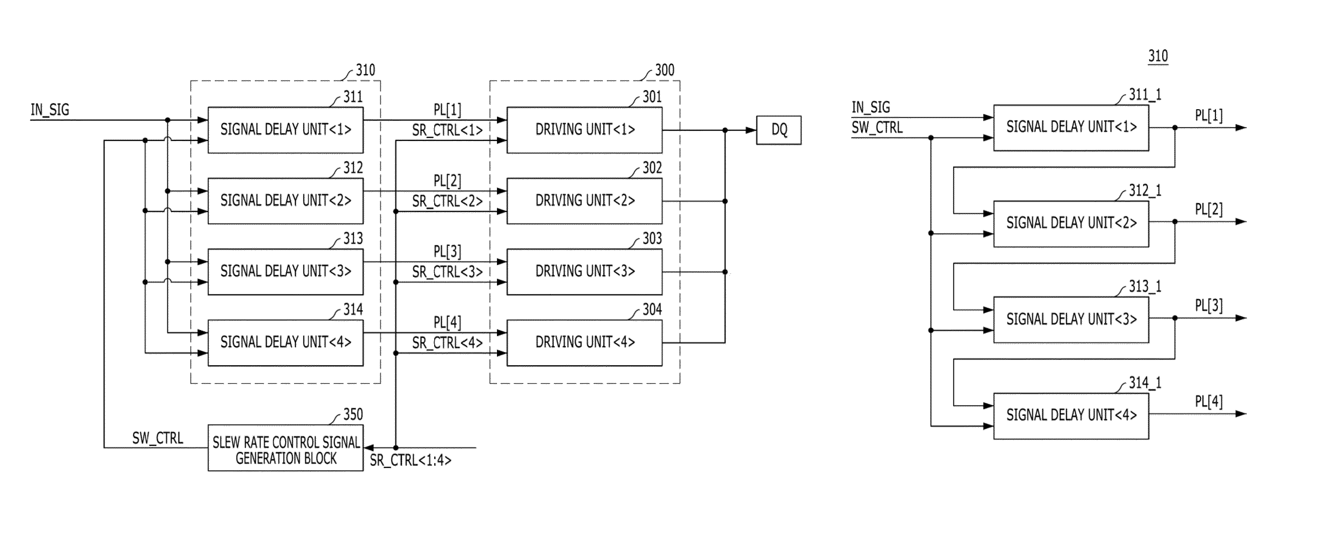
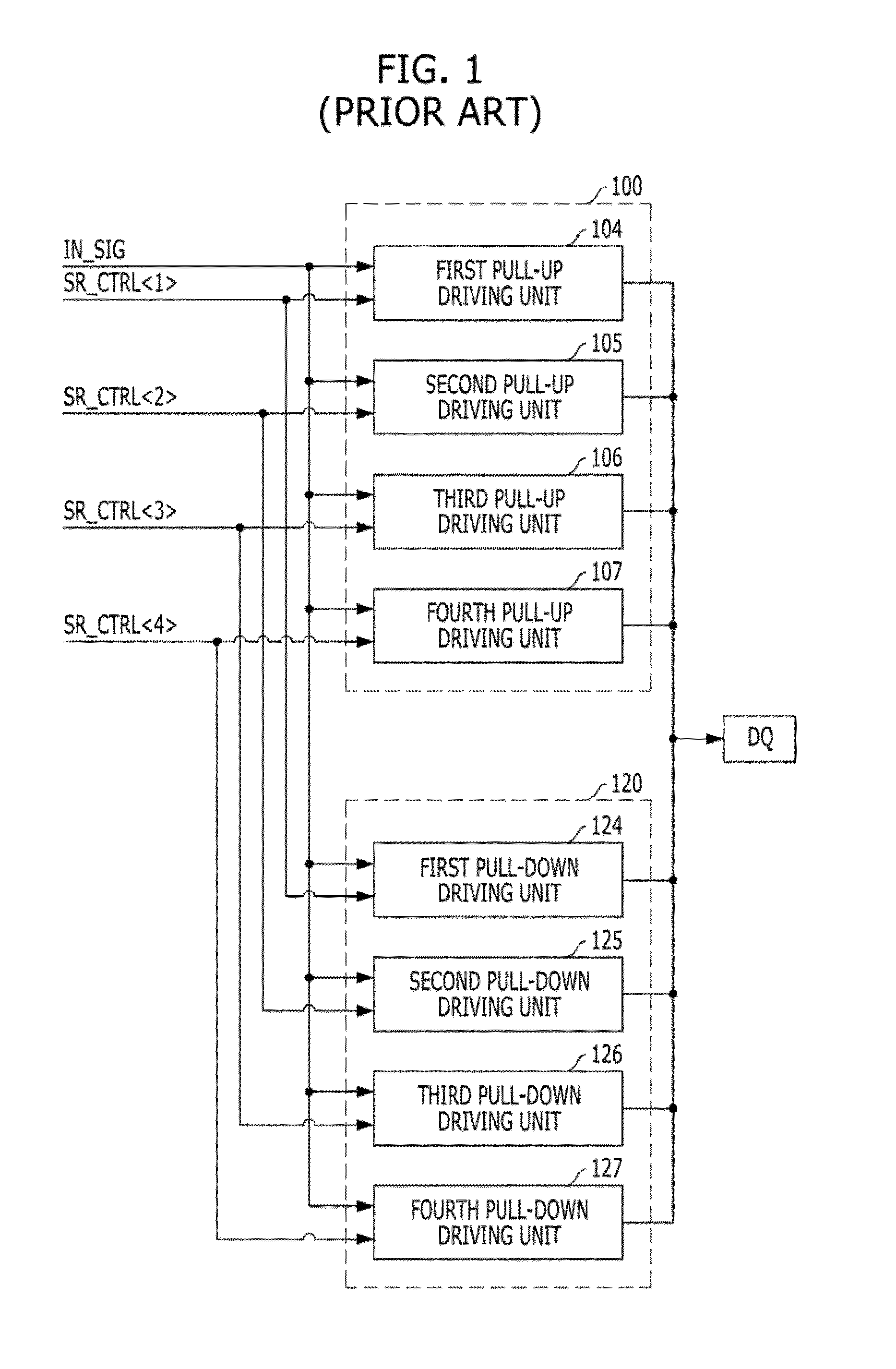
[0037]FIG. 3A is a block diagram illustrating a data output circuit of a low-power semiconductor device, in accordance with a first embodiment of the present invention.

[0038]Referring to FIG. 3A, the data output circuit of the low-power semiconductor device, in accordance with a first embodiment of the present invention, includes a driving operation block 300, and slew rate control blocks 310 and 350. The slew rate control blocks 310 and 350 include a signal delay operation block 310, and a slew rate control signal generation block 350.

[0039]The driving operation block 300 is configured to drive an output node DQ to a logic high level, corresponding to a power supply voltage (VDD), based on logic high levels of inputted signals PL[1:4], and drive the output node DQ to a logic low level, corresponding to a ground voltage (VSS), based on logic low levels of the inputted signals PL[1:4].

[0040]The driving operation block 300 includes a plurality of driving units 301, 302, 303 and 304. T...

second embodiment

[0071]FIG. 4A is a block diagram illustrating a data output circuit of a low-power semiconductor device, in accordance with a second embodiment of the present invention.

[0072]Referring to FIG. 4A, the data output circuit of the low-power semiconductor device, in accordance with a second embodiment of the present invention, includes a first driving operation block 400, a second driving operation block 420, and slew rate control blocks 410, 430 and 450. The slew rate control blocks 410, 430 and 450 include a first signal delay operation block 410, a second signal delay operation block 430, and a slew rate control signal generation block 450.

[0073]The first driving operation block 400 is configured to drive an output node DQ to a logic high level, corresponding to a power supply voltage (VDD), based on logic high levels of inputted signals PU[1:4], or drive the output node DQ to a logic low level, corresponding to a ground voltage (VSS), based on logic low levels of the inputted signal...


PUM


Abstract

A semiconductor device includes a plurality of driving units configured to drive an output node based on an input signal and be on / off controlled based on driving force control codes, respectively, a slew rate control signal generation block configured to generate a slew rate control signal based on the driving force control codes, and a plurality of signal delay units configured to delay the input signal by respectively different delay amounts, transfer resultant signals to the plurality of driving units, and be respectively controlled in their delay amounts based on the slew rate control signal.

Description

CROSS-REFERENCE TO RELATED APPLICATIONS[0001]The present application claims priority of Korean Patent Application No. 10-2012-0150008, filed on Dec. 20, 2012, which is incorporated herein by reference in its entirety.BACKGROUND[0002]1. Field[0003]Exemplary embodiments of the present invention relate to a semiconductor design technology, and more particularly, to an output circuit of semiconductor device.[0004]2. Description of the Related Art[0005]In general, in a low-power semiconductor device (i.e., designed to operate under low power condition), an output circuit is desirable to reduce power consumption, and due to this fact, it may be difficult to secure signal integrity of output signal.[0006]For example, in a main memory or a graphic memory, which has no limitation in terms of power consumption, a termination control circuit such as an on-die termination (ODT) circuit is included to be connected to a data output terminal to suppress reflective waves when transmitting data, the...

Claims


Application Information

Patent Timeline
Patent Type & Authority Patents(United States)
IPC IPC(8): H03K3/01H03K5/12
CPCH03K3/01H03K19/00361G11C7/22G11C7/10
Inventor SHON, KWAN-SUSONG, TAEK-SANG
Owner SK HYNIX INC
Why Eureka
Try Eureka