Method for fabricating backside-illuminated sensors

a technology of backside illumination and sensor, which is applied in the direction of photovoltaic energy generation, electrical equipment, semiconductor devices, etc., can solve the problems of more shadowing, crosstalk and denser circuitry wiring, and increasing pixel density

Inactive Publication Date: 2014-10-28
NEUTRON THERAPEUTICS LLC
View PDF22 Cites 0 Cited by
  • Summary
  • Abstract
  • Description
  • Claims
  • Application Information

AI Technical Summary

Problems solved by technology

However, increasing pixel density creates issues such as crosstalk and denser circuitry wiring.
Increasing the amount of wiring causes more shadowing and therefore less efficiency of light reaching the silicon light-sensitive layer.
However, BSI sensors require thinner silicon in order for the light to pass through and reach the photoactive layer and therefore have not been as cost-effective to manufacture as FSI sensors.
BSI sensors also require precision uniformity in thickness across the chip, which can be difficult to accomplish.
Because it is difficult to achieve the necessary precision uniformity in thickness with grinding, BSI processing often requires both wafer level grinding and die level polishing.
This creates throughput issues, increases cost, and can cause contamination.

Method used


Image

  • Method for fabricating backside-illuminated sensors
  • Method for fabricating backside-illuminated sensors
  • Method for fabricating backside-illuminated sensors

Examples


Embodiment Construction

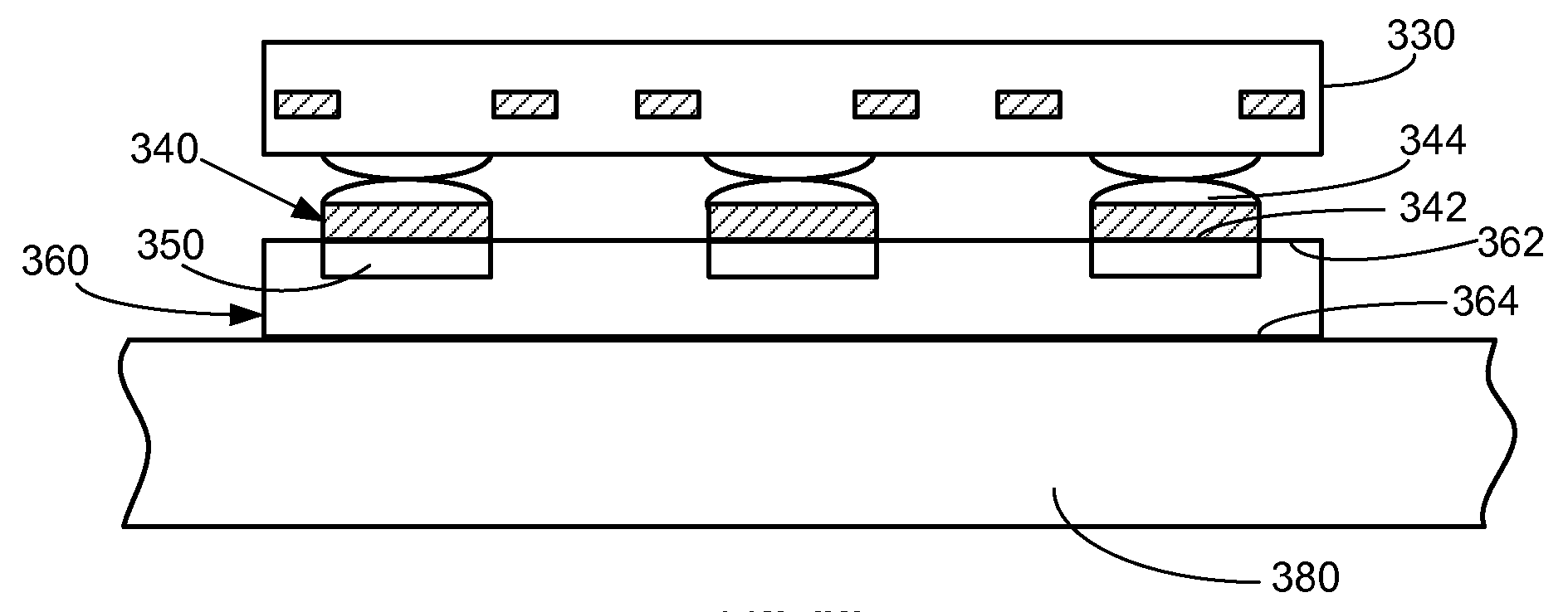
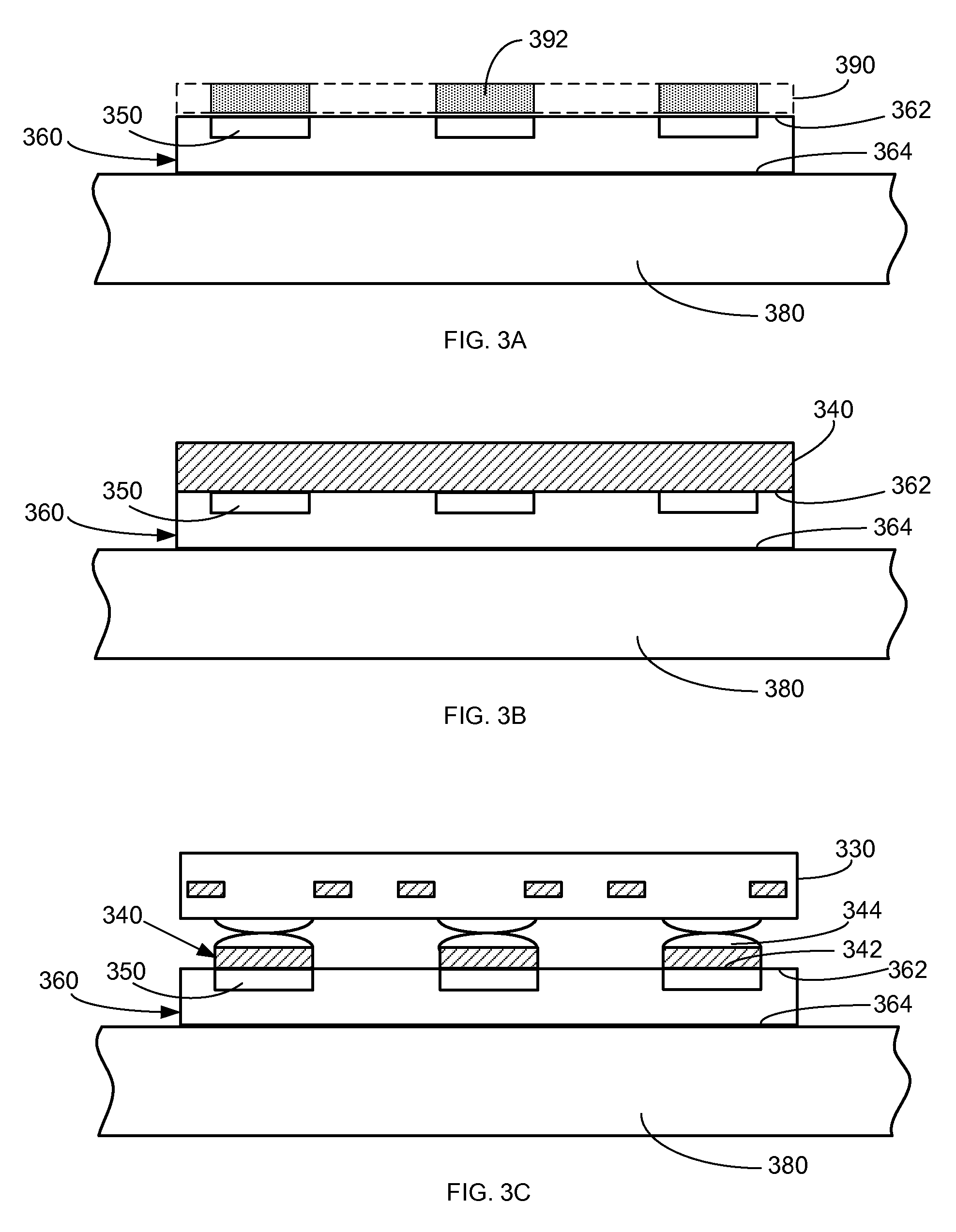
[0014]A backside-illuminated sensor is fabricated using a lamina having a thickness substantially equivalent to the desired thickness for the finished sensor device. In some embodiments, the lamina may be provided as a free-standing lamina, in which doped regions are formed within and at a front surface of the lamina. In other embodiments, doped regions are formed in a first surface of a semiconductor donor body and a lamina is cleaved from the donor body, where the doped regions are within and at the front surface of the lamina. The methods disclosed herein enable improving throughput and decreasing manufacturing cost.

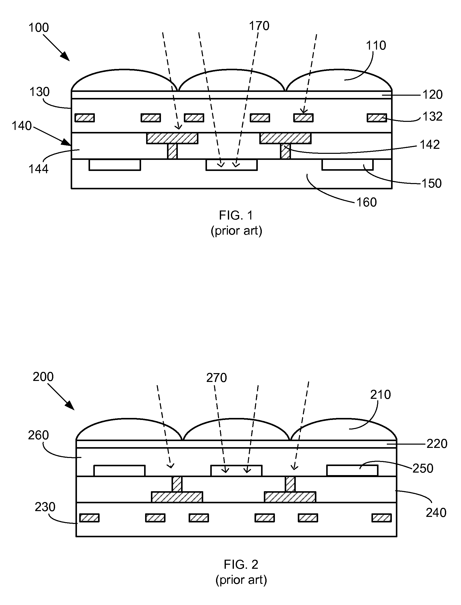
[0015]FIG. 1 shows a simplified view of a conventional FSI sensor 100 which includes lenses 110, color filter 120, integrated circuit 130, metal interconnect layer 140, doped regions 150 and semiconductor substrate 160. The semiconductor substrate 160 has a first conductivity and may be, for example, silicon. The doped regions 150 are doped to a different conductivity...


PUM


Abstract

A method for fabricating a backside-illuminated sensor includes providing a thin film semiconductor lamina having a first conductivity, and forming a doped region having a second conductivity within the lamina and at a front surface of the lamina. The lamina may be provided as a free-standing lamina, or may be provided as a semiconductor donor body from which the lamina is cleaved. An electrical connection is formed to the doped region. A temporary carrier is contacted to the back surface of the semiconductor and later removed. A backside-illuminated sensor is fabricated from the semiconductor lamina, in which the thickness of the semiconductor lamina remains substantially unchanged during the fabrication process.

Description

RELATED APPLICATIONS[0001]This application claims priority to U.S. Provisional Application No. 61 / 596,694, filed Feb. 8, 2012, and entitled “Method for Fabricating Backside-Illuminated Sensors,” which is hereby incorporated by reference for all purposes. This application is also related to Zuniga, U.S. patent application Ser. No. 13 / 425,870 entitled “Back-Contact Photovoltaic Cell Comprising A Thin Lamina Having A Superstrate Receiver Element,” filed on Mar. 21, 2012, and which is hereby incorporated by reference for all purposes.BACKGROUND OF THE INVENTION[0002]Image sensors receive light and convert the energy into electrical signals based on the amount of light received. Image sensors generally include a silicon light-sensitive layer and electrical circuitry, such as an integrated chip, for processing the electrical signals. It is desirable to increase the pixel density on a chip to improve resolution. However, increasing pixel density creates issues such as crosstalk and denser ...

Claims


Application Information

Patent Timeline
Patent Type & Authority Patents(United States)
IPC IPC(8): H01L31/0232
CPCH01L27/14687H01L31/1896H01L31/103Y02E10/50H01L27/1464H01L27/14632H01L21/6835
Inventor MURALI, VENKATESANCHARI, ARVINDPRABHU, GOPALPETTI, CHRISTOPHER J.
Owner NEUTRON THERAPEUTICS LLC
Why Eureka
Try Eureka