Multilayer laminate package and method of manufacturing the same

a technology of laminated packages and electronic components, applied in the direction of printed electric component incorporation, association of printed circuit non-printed electric components, electrical apparatus construction details, etc., can solve the problems of poor electrical properties, thin and small, and inability to ensure the reworkability of faulty electronic components, so as to achieve high reworkability and yield

Inactive Publication Date: 2014-10-28
SAMSUNG ELECTRONICS CO LTD
View PDF19 Cites 18 Cited by
  • Summary
  • Abstract
  • Description
  • Claims
  • Application Information

AI Technical Summary

Benefits of technology

[0008]The following description relates to a multilayer laminate package and a method of manufacturing the same, which can guarantee high reworkability and yield.
[0009]The following description also relates to a multilayer laminate package and a method of manufacturing the same, which can make nearly all types of electronic components embeddable and contribute to the reduction of the weight, thickness and size of information technology (IT) devices and the improvement of the performance of IT devices.

Problems solved by technology

As the performance of information technology (IT) devices is improved, mobile IT devices are becoming light-weighted, thin and small.
The ‘during lamination’ embedding technique, which is characterized by embedding electronic components during the lamination of the layers of a core layer and / or a build-up layer of a multilayer laminate package, can provide excellent electrical properties, but fails to ensure a high yield of electronic devices and reworkability for faulty electronic components.
On the other hand, the ‘after lamination’ embedding technique, which is characterized by embedding electronic components after the lamination of the layers of a core layer and / or a build-up layer of a multilayer laminate package, can provide a high yield of electronic devices and high reworkability, but can be responsible for poor electrical properties, which causes disadvantages given that it is required to ensure excellent electrical properties between the layers of a core layer or a build-up layer of a multilayer laminate package and between the core layer and the build-up layer.

Method used


Image

  • Multilayer laminate package and method of manufacturing the same
  • Multilayer laminate package and method of manufacturing the same
  • Multilayer laminate package and method of manufacturing the same

Examples


Embodiment Construction

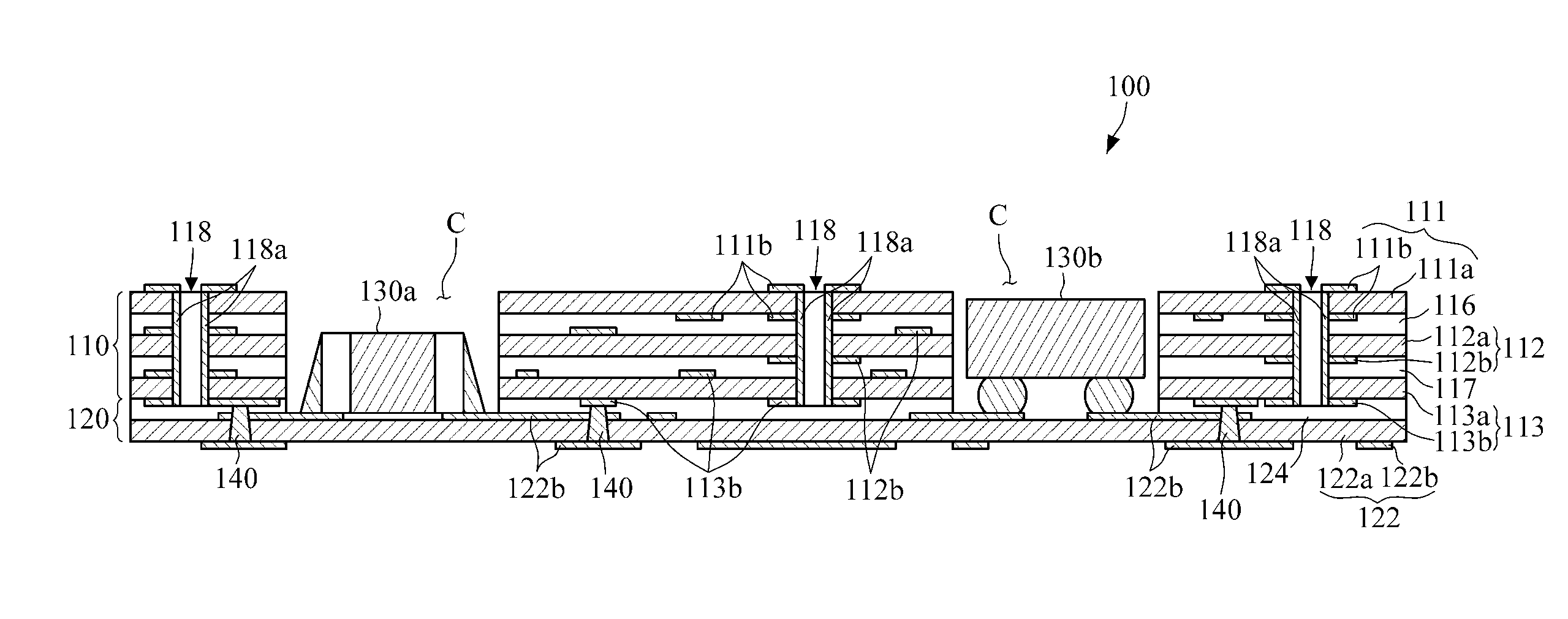
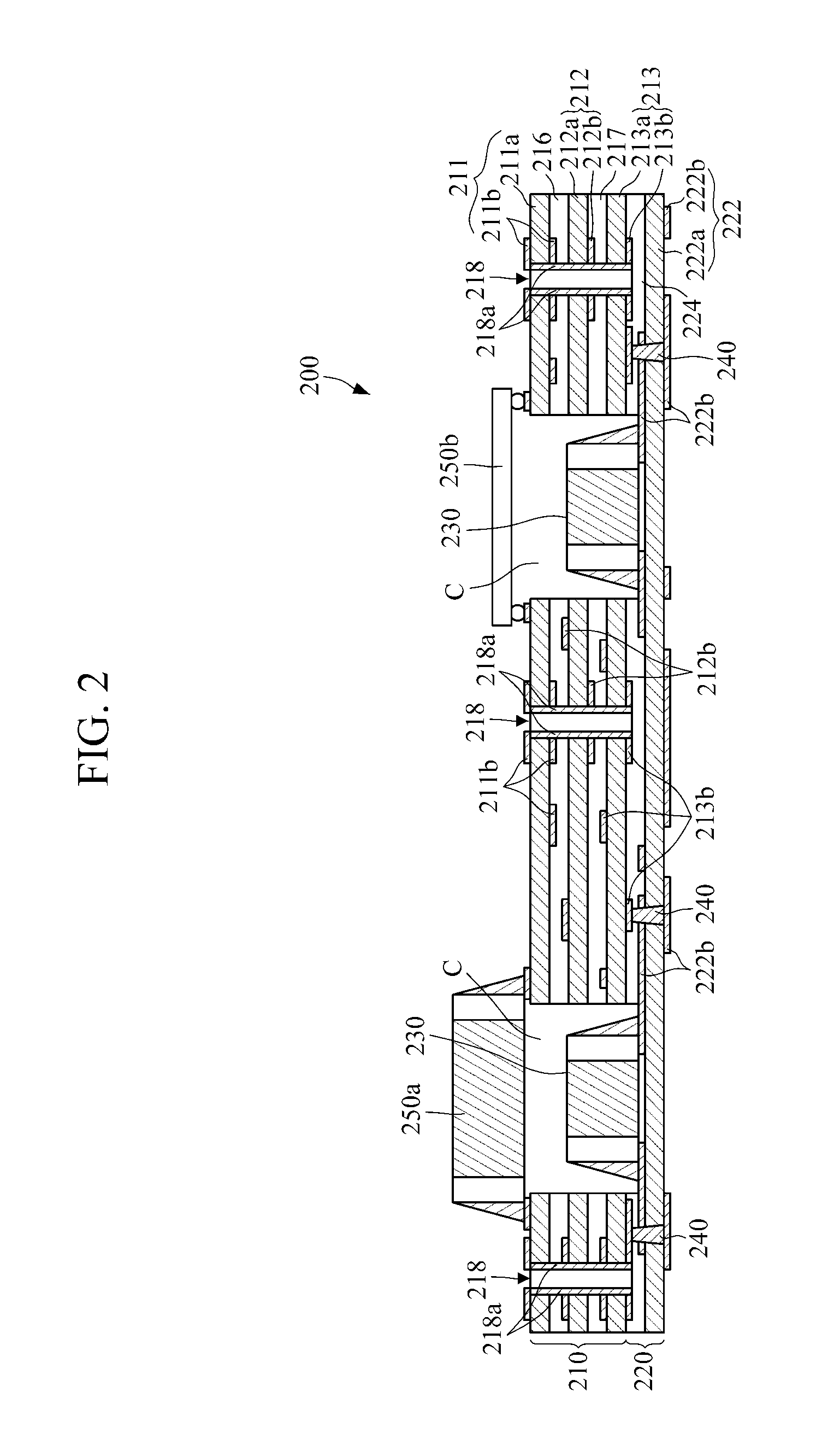
[0021]The following description is provided to assist the reader in gaining a comprehensive understanding of the methods, apparatuses, and / or systems described herein. Accordingly, various changes, modifications, and equivalents of the methods, apparatuses, and / or systems described herein will be suggested to those of ordinary skill in the art. Also, descriptions of well-known functions and constructions may be omitted for increased clarity and conciseness.

[0022]Multilayer laminate packages according to exemplary embodiments can be suitable for use not only in information technology (IT) devices (particularly, mobile IT devices such as a mobile phone) but also in bio-healthcare electronic devices and wearable electronic devices as a system integration package technology. For example, the multilayer laminate packages according to exemplary embodiments can be applied to mobile devices (such as mobile phones, including smart phones, personal digital assistants (PDAs), or portable multi...


PUM

PropertyMeasurementUnit
thicknessaaaaaaaaaa
electricallyaaaaaaaaaa
electrically insulatingaaaaaaaaaa

Abstract

A multilayer laminate package and a method of manufacturing the same are provided. The multilayer laminate package includes a cavity layer, a non-cavity layer, an electronic component, and a metalized blind via. The cavity layer includes a first adhesive layer and two first circuit layers, which are stacked with the first adhesive layer between, and an opening. The non-cavity layer includes a second adhesive layer and a second circuit layer. The non-cavity layer is bonded to the cavity layer with the second adhesive layer so as to close one side of the opening. The electronic component is mounted in the opening and is electrically connected to the non-cavity layer exposed through the opening. The metalized blind via electrically connects the non-cavity layer to one of the circuit layers of the cavity layer.

Description

CROSS-REFERENCE TO RELATED APPLICATION(S)[0001]This application claims priority under 35 U.S.C. §119(a) of Korean Patent Application No. 10-2010-0074321, filed on Jul. 30, 2010, in the Korean Intellectual Property Office, the entire disclosure of which is incorporated by reference herein for all purposes.BACKGROUND[0002]1. Field[0003]The following description relates to packaging technology for electronic components, and particularly, to embedded package technology for electronic components.[0004]2. Description of the Related Art[0005]As the performance of information technology (IT) devices is improved, mobile IT devices are becoming light-weighted, thin and small. Further, with the integration of various types of modules into a single electronic device becoming widespread, embedded package technology, which is capable of embedding various electronic components (such as an integrated circuit (IC) chip, a capacitor, a resistor, an inductor, an antenna, a micro-electro-mechanical-sys...

Claims


Application Information

Patent Timeline
Patent Type & Authority Patents(United States)
IPC IPC(8): H05K7/00H05K1/16H05K3/46H05K7/02H05K1/18
CPCH05K3/462H01L2224/16225H05K1/186H01L2924/1461Y10T29/4913Y10T29/49165H01L2924/00
Inventor LEE, BAIK-WOOLIM, JI-HYUKBOOH, SEONG-WOON
Owner SAMSUNG ELECTRONICS CO LTD
Why Eureka
Try Eureka