

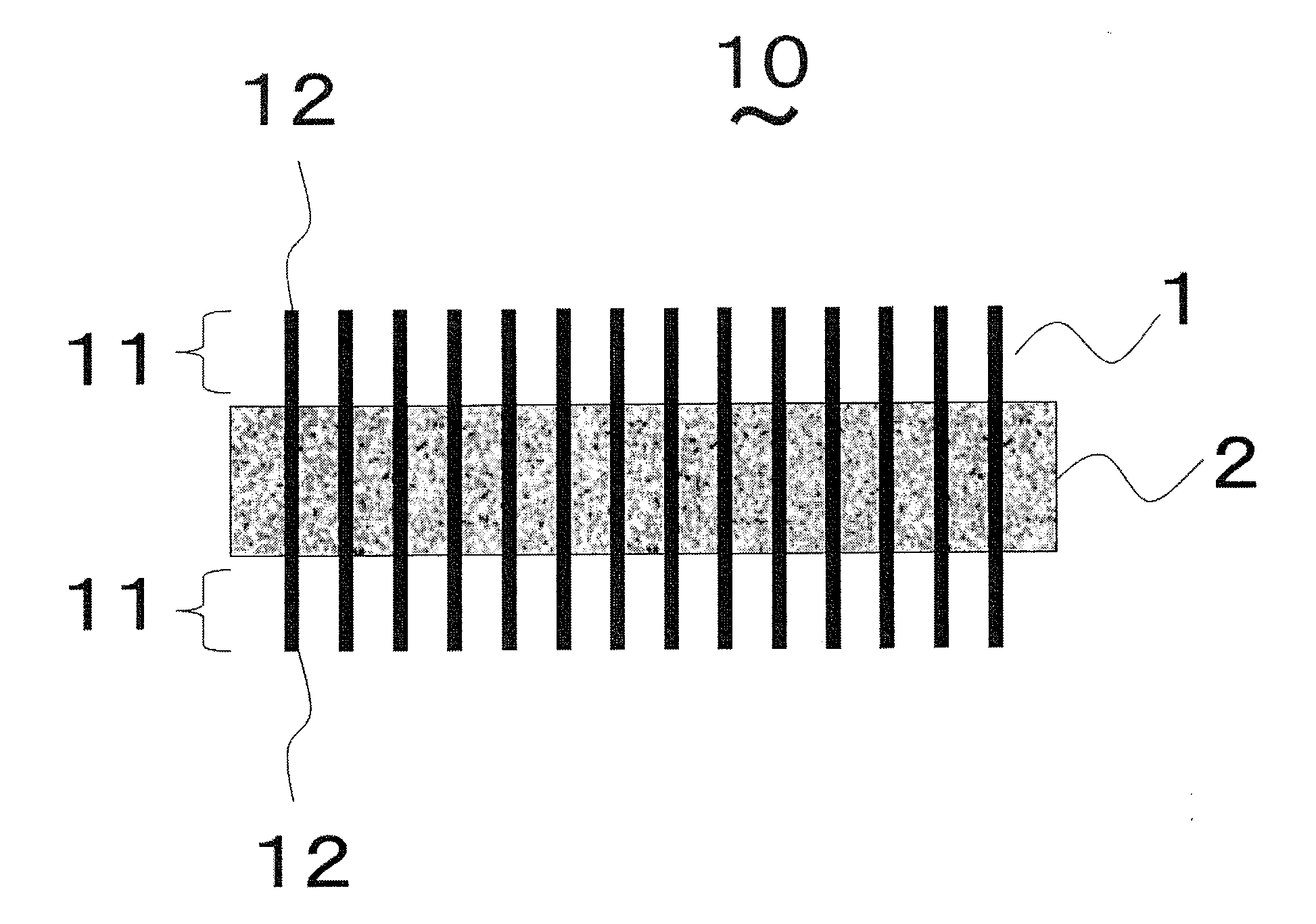
Carbon nanotube aggregate
a carbon nanotube and aggregate technology, applied in the direction of non-metal conductors, instruments, conductors, etc., can solve the problems of insufficient thermal diffusion property and high conductivity of composite materials, and achieve the effect of high thermal diffusion property, sufficient adhesive strength, and high conductivity
- Summary
- Abstract
- Description
- Claims
- Application Information
AI Technical Summary
Benefits of technology
Problems solved by technology
Method used
Image

Examples
production example 1
Preparation of UV-Curable Resin Syrup
[0093]UV-curable resin syrup was prepared by adding 0.05 part of an IRGACURE 651 (manufactured by Ciba Specialty Chemicals) and 0.05 part of an IRGACURE 184 (manufactured by Ciba Specialty Chemicals) as photopolymerization initiators to 100 parts of an EBECRYL 3701 (manufactured by DAICEL-CYTEC Company, Ltd.).
example 1
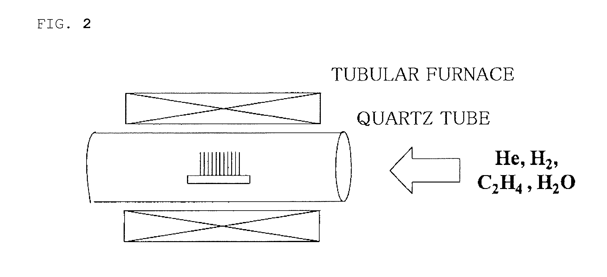
[0094]An Al thin film (having a thickness of 10 nm) was formed on a silicon substrate (manufactured by ELECTRONICS AND MATERIALS CORPORATION, thickness: 525 μm) with a vacuum evaporator (manufactured by JEOL Ltd., JEE-4X Vacuum Evaporator). After that, the resultant was subjected to an oxidation treatment at 450° C. for 1 hour. Thus, an Al2O3 film was formed on the silicon substrate. An Fe thin film (having a thickness of 1 nm) was further deposited from the vapor onto the Al2O3 film with a sputtering apparatus (manufactured by ULVAC, Inc., RFS-200). Thus, a catalyst layer was formed.
[0095]Next, the silicon substrate with the catalyst layer was cut and mounted in a quartz tube having a diameter of 30 mm. A mixed gas of helium and hydrogen (120 / 80 sccm) with its moisture content kept at 350 ppm was flowed into the quartz tube for 30 minutes so that the air in the tube was replaced. After that, the temperature in the tube was increased to 765° C. with an electric tubular furnace in 35...
example 2
[0102]An Al thin film (having a thickness of 10 nm) was formed on a silicon substrate (wafer with a thermal oxide film, manufactured by KST, 1,000 μm) with a vacuum evaporator (manufactured by JEOL Ltd., JEE-4X Vacuum Evaporator). After that, the resultant was subjected to an oxidation treatment at 450° C. for 1 hour. Thus, an Al2O3 film was formed on the silicon substrate. An Fe thin film (having a thickness of 2 nm) was further deposited from the vapor onto the Al2O3 film with a sputtering apparatus (manufactured by ULVAC, Inc., RFS-200). Thus, a catalyst layer was formed.
[0103]Next, the silicon substrate with the catalyst layer was cut and mounted in a quartz tube having a diameter of 30 mm. A mixed gas of helium and hydrogen (120 / 80 sccm) with its moisture content kept at 350 ppm was flowed into the quartz tube for 30 minutes so that the air in the tube was replaced. After that, the temperature in the tube was increased to 765° C. with an electric tubular furnace in 35 minutes i...
PUM
| Property | Measurement | Unit |
|---|---|---|
| length | aaaaa | aaaaa |
| length | aaaaa | aaaaa |
| length | aaaaa | aaaaa |
Abstract
Description
Claims
Application Information